Structure and driving method for active photoelectric element

a photoelectric element and driving method technology, applied in the direction of instruments, static indicating devices, etc., can solve the problems of image residual, difficult to control gray scale, high manufacturing cost of array substrates, etc., to reduce the number of ics, and reduce the number of channels

Inactive Publication Date: 2009-12-08
WINTEK CORP
View PDF8 Cites 0 Cited by
  • Summary
  • Abstract
  • Description
  • Claims
  • Application Information

AI Technical Summary

Benefits of technology

[0009]Consequently, the main purpose of the present invention is to reduce half number of channels, compared with the traditional method that uses a pair of select lines to drive a pixel, by way of the unsymmetrical configuration for two sets of thin film diodes and the up / down pixels sharing one select line and collocating corresponding driving voltages. Reducing the number of channels will reduce the number of ICs. The following manufacturing process for IC bonding for panels becomes more convenient, the manufacturing cost is lowered effectively, the manufacturing difficulty is reduced, and the design complexity is also decreased.
[0010]Another purpose of the present invention is that the current invention reduces the quantity of channels effectively. Reducing the quantity of channels will promote the whole aperture rate and resolution.
[0011]The third purpose of the present invention is that the current invention reduces the quantity of channels effectively whereas the well-known problem of incomplete etching due to parallel arranged two select lines such that the yield rates can be promoted.

Problems solved by technology

However, normally there are at least five steps of mask in the manufacturing process for a TFT array substrate so the manufacturing cost of an array substrate is higher than a traditional passive-matrix LCD.
However, a traditional MIM LCD has the problems of image residual and not easy to control the gray scale.
The method of using two scan lines to drive one pixel solves the problems of image residual and not easy to control the gray scale for a traditional MIM LCD.
Moreover, the following manufacturing process for IC bonding becomes a big problem because the quantity of whole channel increased.
As a result, not only the circuit design becomes more complicated that affects the yield rates but also the needed IC parts are increased that increase the manufacturing cost.

Method used


Image

  • Structure and driving method for active photoelectric element
  • Structure and driving method for active photoelectric element
  • Structure and driving method for active photoelectric element

Examples


Embodiment Construction

[0019]The detailed descriptions for content and technology of the present invention associate with figures are as follows.

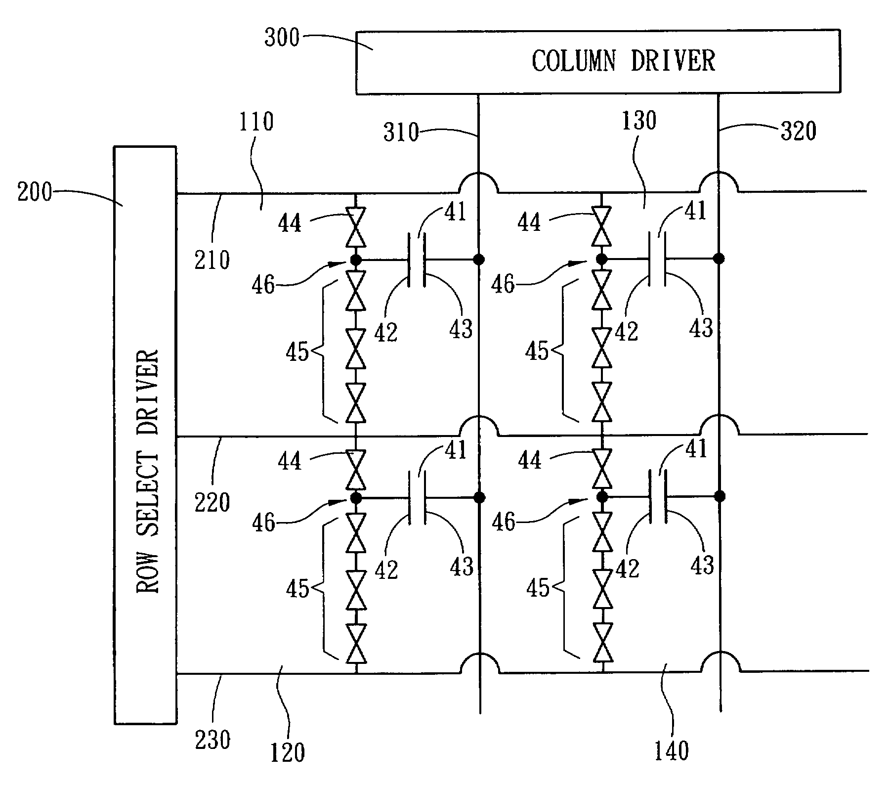
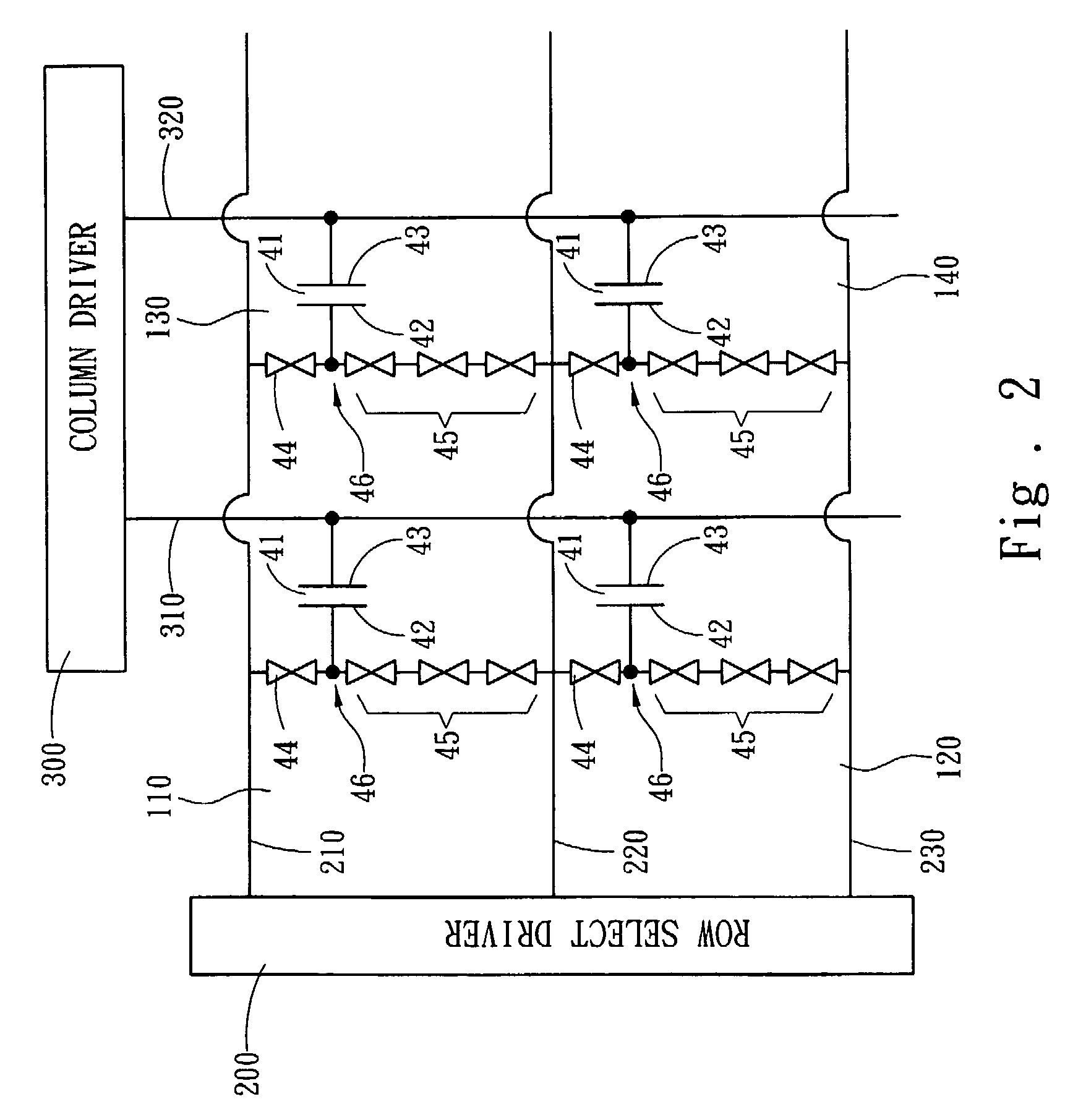
[0020]Please refer to FIG. 2, which is the schematic diagram for the specific circuit design for the 2×2 active matrix panel of the present invention. Data lines 310 and 320 connect to a column-driving element 300, and select lines 210, 220, and 230 connect to a row-selecting element. All the data lines 310 and 320 are arranged as a column configuration and parallel to one another on the panel, all the select lines 210, 220, and 230 are arranged as a row configuration and parallel to one another on the panel. All the data lines 310, 320 and all the select lines 210, 220, and 230 are perpendicular to one another on the panel such that they crisscross construct pixels 110, 120, 130, and 140. Plural active matrix-arranged pixels 110, 120, 130, and 140 are thus constructed on the panel.

[0021]Each pixel of the matrix-arranged pixels 110, 120, 130, and 140 includes a c...


PUM


Abstract

A structure and driving method for active photoelectric element that aims to every matrix-arranged pixel on the display panel. The pixel structure includes a set of first thin film diodes and a set of second thin film diodes. The first set and the second set of film diodes are connected at a node. The electrical impedances of the first set and the second set of film diodes are unsymmetrical. The first set of film diodes connects to the select lines of the pixel while the second set of film diodes connects to the select lines of the pixel on the next row, which forms a configuration that the up / down pixels share one select line. Consequently, the driving signal for the up select line of a single pixel is determined by the driving signal for the down select line of the up pixel so as to reduce the quantity of select lines.

Description

FIELD OF THE INVENTION[0001]The present invention relates to a structure and driving method for an active photoelectric element. By way of the unsymmetrical configuration for diodes and the up / down pixels share one select line in a single pixel, and collocating corresponding driving voltages to achieve the goals of voltage control and driving the liquid crystal to rotate.BACKGROUND OF THE INVENTION[0002]Compared a Thin Film Transistor Liquid Crystal Display (TFT LCD) with a Twisted-Nematic (TN) LCD or a Supertwisted-Nematic (STN) LCD, a TFT LCD is active driving so it has merits like good image quality, and quick response time. Therefore, TFT LCDs become the main fashion of LCDs gradually.[0003]However, normally there are at least five steps of mask in the manufacturing process for a TFT array substrate so the manufacturing cost of an array substrate is higher than a traditional passive-matrix LCD.[0004]Accordingly, people started to develop that using Metal-Insulator-Metal (MIM) th...

Claims


Application Information

Patent Timeline
Patent Type & Authority Patents(United States)
IPC IPC(8): G09G3/36
CPCG09G3/367G09G2300/0809G09G2300/0465
Inventor WANG, WEN-CHUNKANG, HENTAWANG, YI-CHIN
Owner WINTEK CORP
Why Eureka
Try Eureka