Reverse side film laser circuit etching

a laser circuit and side film technology, applied in laser beam welding apparatus, printed circuit dielectrics, transparent dielectrics, etc., can solve the problems of slow circuit etching methods that use chemicals, coatings and acids, and high cost, and achieve low cost per unit, easy recycling of metals, and low cost per unit

Inactive Publication Date: 2009-12-15
MU GAHAT HLDG
View PDF32 Cites 29 Cited by
  • Summary
  • Abstract
  • Description
  • Claims
  • Application Information

AI Technical Summary

Benefits of technology

[0012]An advantage of the present invention is that a system is provided that can produce RFID circuits on flexible printed circuits at exceedingly low cost per unit.
[0013]Another advantage of the present invention is manufacturing method is provided that produces very little waste and that readily recycles the metals ablated from the tapes.
[0014]A further advantage of the present invention is manufacturing method for flexible printed circuits is provided for continuous production.

Problems solved by technology

But mass produced commodity items need tags that cost only a few cents.
Circuit etching methods that use chemicals, coatings, and acids are slow, expensive, and not environmentally friendly.

Method used


Image

  • Reverse side film laser circuit etching
  • Reverse side film laser circuit etching
  • Reverse side film laser circuit etching

Examples


Embodiment Construction

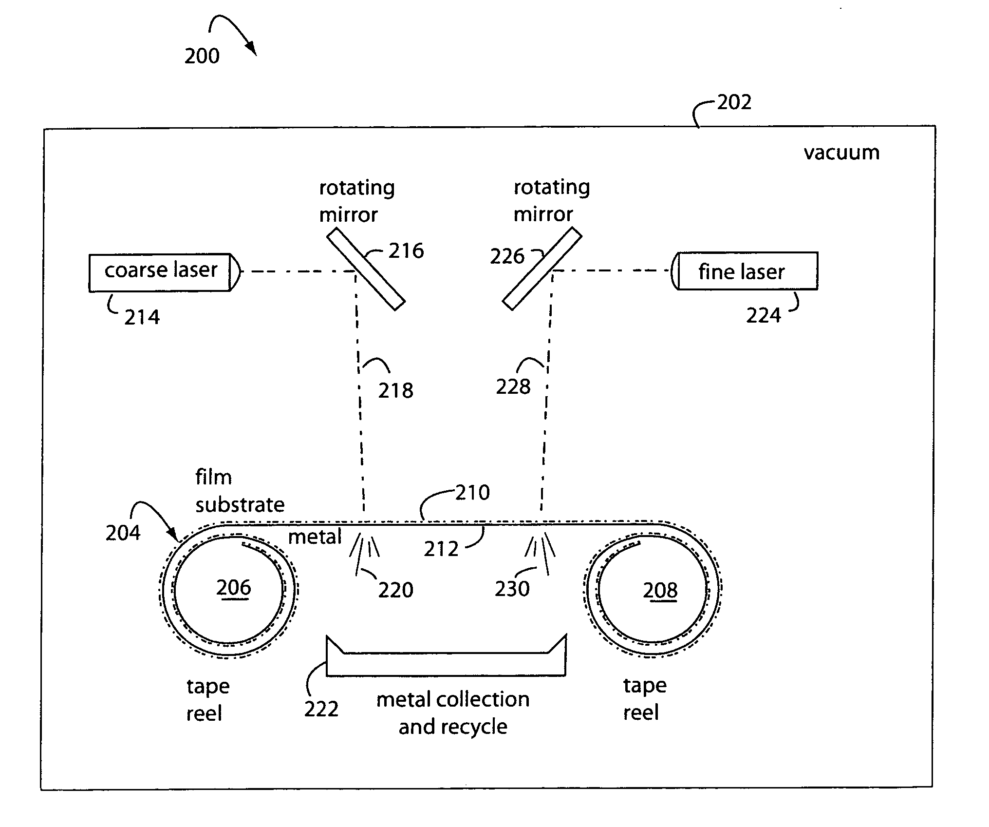
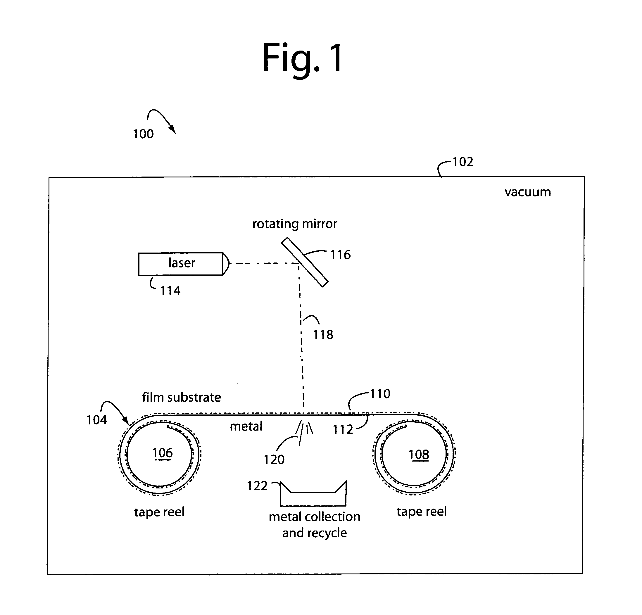
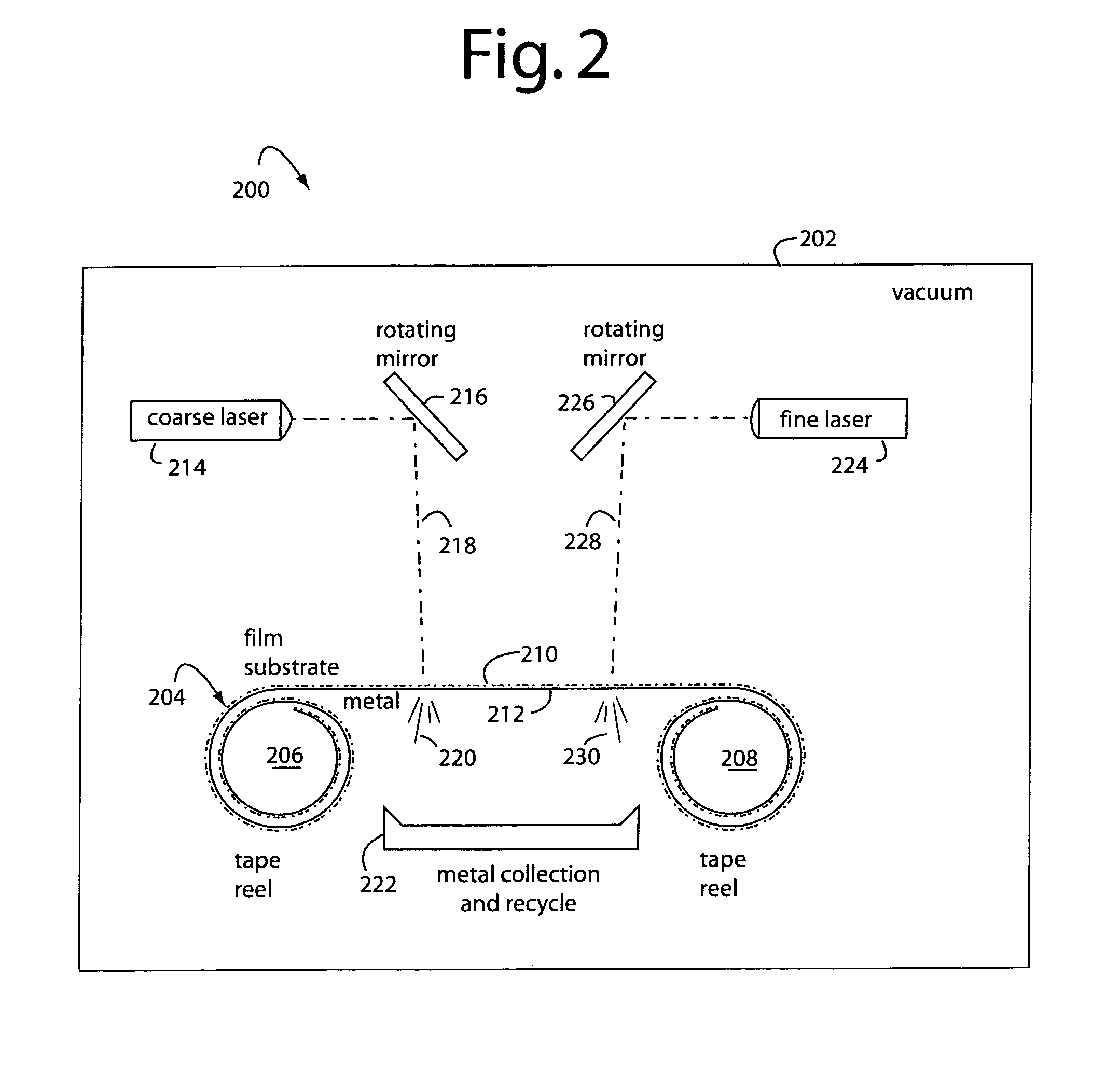
[0020]FIG. 1 represents a direct-write laser lithography system embodiment of the present invention, and is referred to herein by the general reference numeral 100. System 100 is used to manufacture flexible printed circuits (FPC), and comprises a vacuum chamber 102 in which are disposed a metal-on-film substrate tape 104 wound on a supply reel 106 and a take-up reel 108. A vacuum of about 115 torr (0.15 atm) is used. The tape 104 has a transparent film substrate 110 and a thin-film metal cladding 112. The transparent film substrate 110 may comprise polyimide, PEN, polyester, polycarbonate, etc. The thin-film metal cladding 112 may include copper (CU), aluminum (AL), platinum (PT), etc.

[0021]A laser 114 is used to ablate off the metal from the backside of tape 104 as it translates from supply reel 106 to take-up reel 108. A mirror 116 moves a laser beam 118 to various lateral points across the tape 104. Once laser beam 118 is positioned properly, a pulse of energy is generated enoug...


PUM

PropertyMeasurementUnit
wavelengthaaaaaaaaaa
gravityaaaaaaaaaa
energyaaaaaaaaaa

Abstract

A direct-write laser lithography system comprises a reel-to-reel feed system in a vacuum chamber that presents the clear film-side of a single-sided metal-clad tape to a laser for direct patterning of the metal. The laser beam is swept laterally across the tape by rotating mirrors, and is intense enough to ablate the metal but not so strong as to destroy the tape substrate. In one instance, two specialized lasers are used, one set to ablate large field areas, and the other tuned to scribe fine features and lines. The ablated metal blows off in a downward direction and is collected for recycling.

Description

BACKGROUND OF THE INVENTION[0001]1. Field of the Invention[0002]The present invention relates to flexible circuits, and in particular to methods, systems, and devices for manufacturing flexible circuits in very high volumes and at very low costs.[0003]2. Description of the Prior Art[0004]Radio frequency identification device (RFID) technology is proliferating everywhere and into everything. Right now, a worldwide effort is stepping into high gear to replace the familiar universal product code (UPC) barcodes on products with RFID tags. The ink and labels used to print UPC barcodes is very inexpensive, and the costs of RFID chips and printed circuit antennas are under a lot of pressure to match them. Large, expensive items, of course, are not price sensitive to the cost of a typical RFID tag. But mass produced commodity items need tags that cost only a few cents.[0005]The majority of printed circuit boards (PCB's) are made by depositing a layer of copper cladding over the entire subst...

Claims


Application Information

Patent Timeline
Patent Type & Authority Patents(United States)
IPC IPC(8): B23K26/38
CPCB23K26/009B23K26/0846B23K26/365B23K26/409H05K3/027H05K2203/1545H05K2201/0108H05K2203/082H05K1/0393B23K26/40B23K26/361B23K2103/172
Inventor KIRMEIER, JOSEF
Owner MU GAHAT HLDG
Why Eureka
Try Eureka