Infrared sensor and manufacturing method thereof

a manufacturing method and sensor technology, applied in the direction of optical radiation measurement, instruments, material analysis, etc., can solve the problems of high manufacturing cost, crosstalk condition, light interference, etc., and achieve the effect of small size and low manufacturing cos

Inactive Publication Date: 2012-04-10
UNIMEMS MFG
View PDF5 Cites 1 Cited by
  • Summary
  • Abstract
  • Description
  • Claims
  • Application Information

AI Technical Summary

Benefits of technology

[0010]The main object of the instant disclosure is to provide an infrared sensor and manufacturing methods thereof, where the infrared sensor can avoid crosstalk condition with high-sensitivity, has a lower manufacturing cost, and smaller in size.
[0014]The infrared sensor of the instant disclosure has several advantages. First, the infrared sensor can be manufactured with mass production at low cost per unit. Secondly, the infrared sensor is constructed to prevent crosstalk condition of the incoming infrared light. Thirdly, the size of the infrared sensor is reduced. In addition, the material costs for the infrared sensor can be reduced effectively. Furthermore, the infrared sensor can be used with miniature devices like cell phones, ear thermometers, sensing devices, and so on.

Problems solved by technology

However, the distance between the infrared filter 6a and the sensing film 31a is often too large, which can lead to light interference known as the crosstalk condition.
Thus, the associated manufacturing cost is high.

Method used


Image

  • Infrared sensor and manufacturing method thereof
  • Infrared sensor and manufacturing method thereof
  • Infrared sensor and manufacturing method thereof

Examples


Embodiment Construction

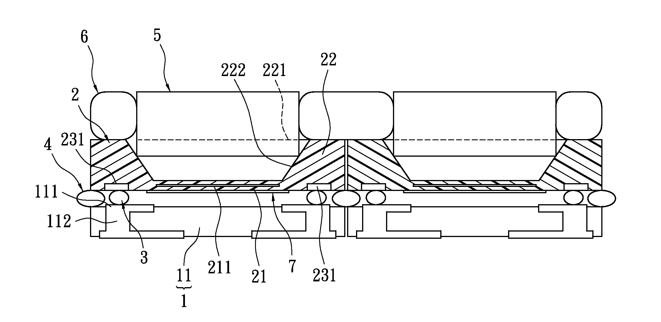
[0026]Please refer to FIG. 7, which shows a cross-sectional view of an infrared sensor for the first embodiment of the instant disclosure. The infrared sensor comprises a substrate 1, a chip 2, a plurality of soldering materials 3, an infrared filter 5, and a reflective layer 7. The soldering materials 3 provide bonding between the substrate 1 and the chip 2, and the infrared filter 5 is disposed onto the chip 2.

[0027]In FIG. 7, the substrate 1 is a circuit board 11 but can be other materials, such as a ceramic plate or a silicon wafer. The circuit board 11 has four contacting members 111 formed on the upper surface thereof. The contacting members 111 also extend downwards in forming four electrical circuits 112, for establishing electrical connection between the top and the bottom surface of the circuit board 11. Based on the operation requirement, the number of the contacting member 111 and the electrical circuit 112 can be varied. The soldering materials 3 are fixed onto the cont...


PUM


Abstract

A manufacturing method for an infrared sensor includes the following steps: providing a wafer having several chips and a substrate; forming four soldering portions, a thermistor, and an infrared sensing layer on the bottom surface of each chip, wherein the soldering portions are connected electrically to the thermistor and the infrared sensing layer; disposing a soldering material onto at least one bonding location for each soldering portion; backside-etching each chip of the wafer to form a sensing film and a surrounding wall around the sensing film; bonding the wafer and the substrate; heating the soldering materials to connect the substrate and each chip of the wafer; disposing an infrared filter on the surrounding wall of each chip; cutting the wafer and the substrate to form a plurality of individual infrared sensors. The instant disclosure further provides an associated infrared sensor.

Description

BACKGROUND OF THE INVENTION[0001]1. Field of the Invention[0002]The instant disclosure relates to an infrared sensor and manufacturing method thereof; in particular, a miniature infrared sensor and the manufacturing method thereof.[0003]2. Description of Related Art[0004]References are made to FIGS. 1 and 2, which illustrate a conventional infrared sensor having a base 1a, a plurality of pins 2a, a chip 3a, a plurality of wires 4a, a cover 5a, an infrared filter 6a, and a thermistor 7a. [0005]The base 1a has a plurality of thru holes 11a. The pins 2a are respectively arranged in the thru holes 11a of the base 1a. The chip 3a has a sensing film 31a in the center location thereon and a surrounding wall 32a surrounding the sensing film 31a. The surrounding wall 32a defines a downward-facing opening 321a in the bottom surface of the chip 3a. The surrounding wall 32a is mounted on the base 1a. The thermistor 7a is disposed on the base 1a. Wires 4a connect the upper surface of the surroun...

Claims


Application Information

Patent Timeline
Patent Type & Authority Patents(United States)
IPC IPC(8): G01J5/00
CPCG01J5/045G01J5/10H01L31/0203H01L2224/48091H01L2924/00014H01L2924/10253H01L2924/00
Inventor LEE, TZONG-SHENG
Owner UNIMEMS MFG
Why Eureka
Try Eureka