Chip type variable electronic part and chip type variable resistor
a technology of electronic parts and resistors, applied in the direction of resistors, resistors with sliding contact, adjustable resistors, etc., can solve the problems of increasing the height of the rotor from the upper surface, increasing the overall height of the chip type variable resistor, incurring an increase in the size of the chip type variable resistor, etc., to achieve the effect of increasing the insertion depth of the screwdriver, effectively reducing the overall height of the chip type variable electronic part,
- Summary
- Abstract
- Description
- Claims
- Application Information
AI Technical Summary
Benefits of technology
Problems solved by technology
Method used
Image
Examples
first embodiment
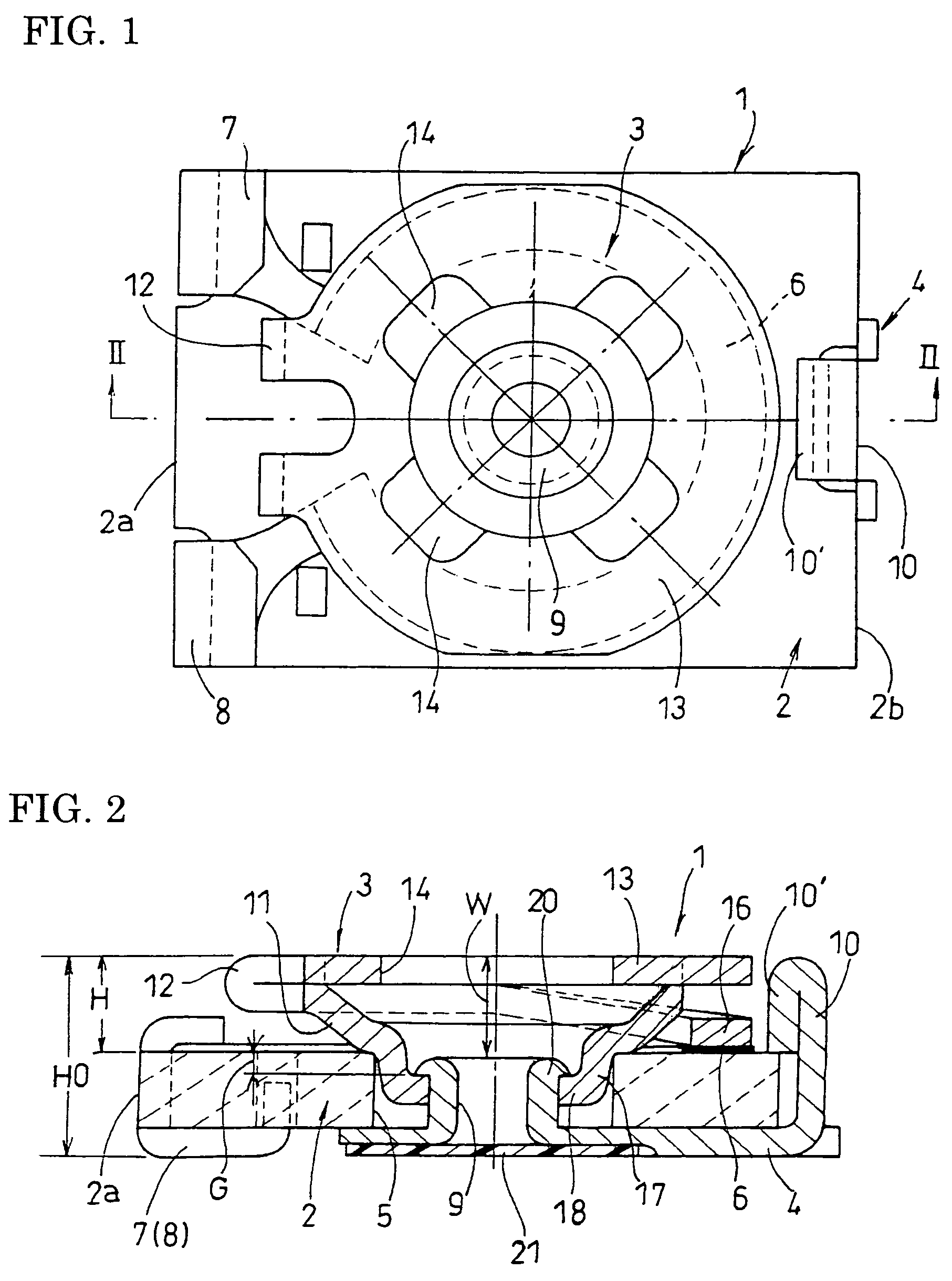
[0052]Among the drawings, FIGS. 1 to 4 depict a chip type variable resistor 1 according to a
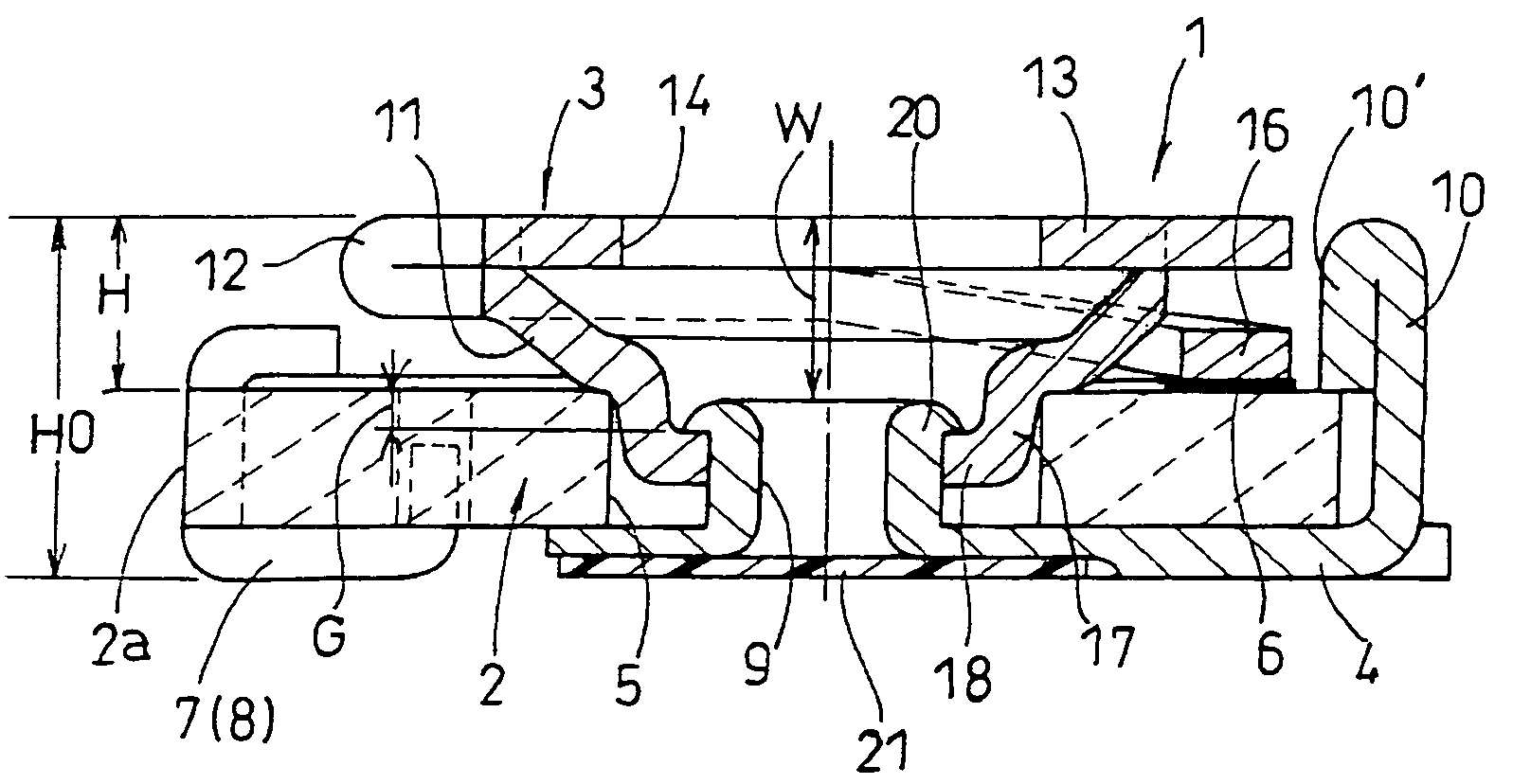
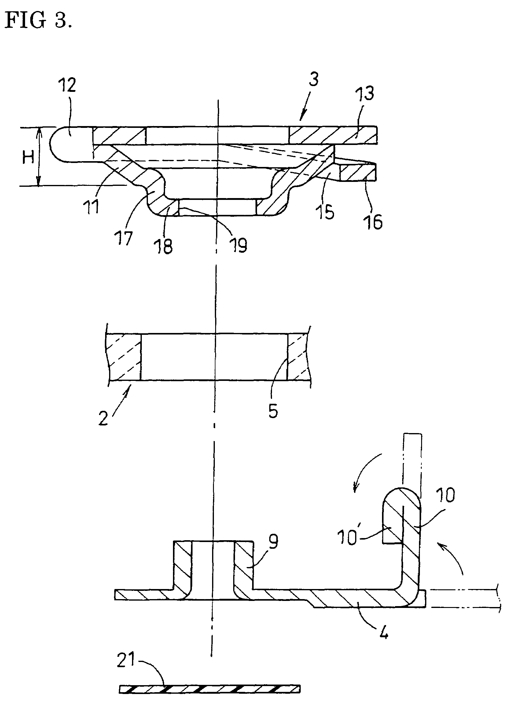
[0053]The chip type variable resistor 1 includes an insulating substrate 2 in the form of a chip made of a heat-resistant insulating material such as a ceramic, an adjustment rotor 3 disposed on the insulating substrate 2, and an internal terminal electrode plate 4 disposed on the lower surface of the insulating substrate 2.
[0054]The insulating substrate 2 is formed with a through hole 5 extending from the upper surface to the lower surface of-the substrate at a generally central position, and a resistance film 6 disposed to extend thereon in an arcuate shape concentric with the through hole 5, and the insulating substrate 2 is provided, on a lateral face 2a thereof, with external terminal electrodes 7, 8 corresponding to the respective end portions of the resistance film 6.
[0055]The internal terminal electrode plate 4 is made of a metal plate and disposed in close contact with the lower surf...
second embodiment
[0065]Now, FIG. 5 depicts a chip type variable resistor according to a
[0066]The second embodiment is based on the configuration in which the bowl shaped first plate 11 of the rotor 3 includes a bottom portion 17 that fits in the through hole 5, and a bottom plate 18 of the bottom portion 17 is placed at a level lower by an appropriate distance G than an uppermost edge of an inner portion of the through hole 5 on the upper surface of the insulating substrate 2, but only the bottom plate 18 out of the bottom portion 17 is brought into contact with the upper surface of the internal terminal electrode plate 4 while the bottom portion 17 is kept from contacting the insulating substrate 2, and the upper end portion of the shaft portion 9 is crimped to extend outward, over the upper surface of the bottom plate 18 thus disposed.
[0067]In such configuration also, the upper end portion 20 of the shaft portion 9 crimped to extend outward is located at a lower level in height than the convention...
third embodiment
[0072]FIG. 6 depicts a chip type variable resistor according to a
[0073]The third embodiment represents a configuration in which a hollow the shaft portion 9′ integrally formed with the internal terminal electrode plate 4 is formed to close the upper end to prevent the intrusion of the flux or the like through the hollow shaft portion 9, instead of adhering the film 21 and forming the fold-back piece 22. Such configuration further ensures prevention of the intrusion of the flux or the like.
PUM
 Abstract
Description
Claims
Application Information


