Robust transistors with fluorine treatment

a transistor and fluorine treatment technology, applied in the field of transistors, can solve the problems of gan based transistor performance limitation, dc and rf characteristics limiting factors, and low breakdown voltage of high current structures, and achieve the effect of high electron mobility

Active Publication Date: 2009-12-29
CREE INC
View PDF39 Cites 115 Cited by
  • Summary
  • Abstract
  • Description
  • Claims
  • Application Information

AI Technical Summary

Problems solved by technology

However, GaAs has a relatively small bandgap (1.42 eV at room temperature) and relatively small breakdown voltage, which prevents GaAs based HEMTs from providing high power at high frequencies.
Electron trapping and the resulting difference between DC and RF characteristics have been a limiting factor in the performance of GaN based transistors, such as AlGaN / GaN HEMTs.
However, due to the high electric fields existing in these structures, charge trapping as well as lower breakdown voltage for high current structures can still be an issue.

Method used


Image

  • Robust transistors with fluorine treatment
  • Robust transistors with fluorine treatment
  • Robust transistors with fluorine treatment

Examples


Embodiment Construction

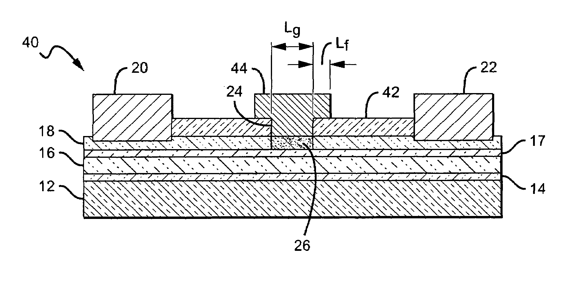
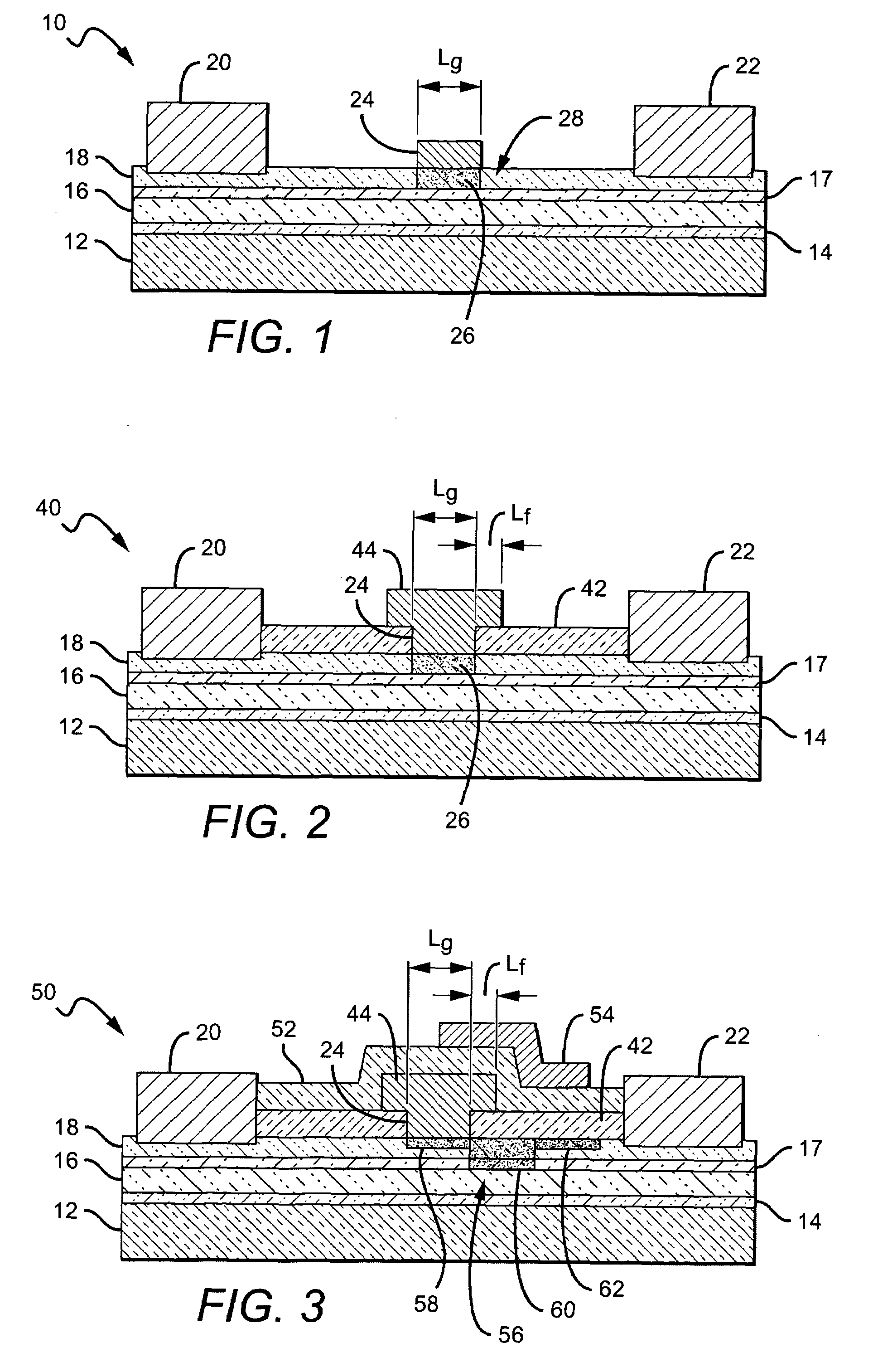
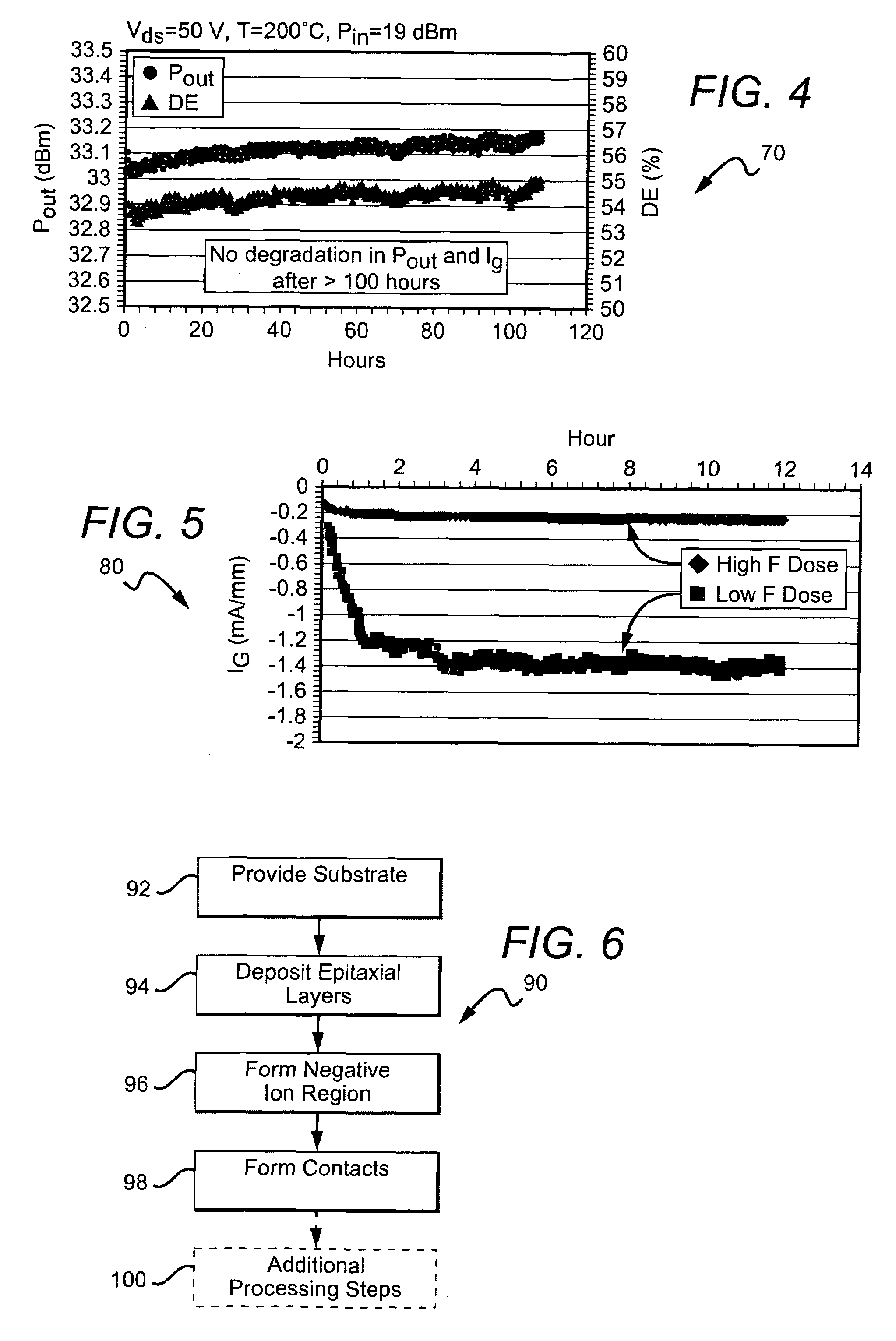
[0023]The present invention relates to semiconductor devices, and in particular transistors, experiencing an electric (E) field during operation. One or more negative ion regions can be included in the device according to the present invention to counter and reduce the transistor's operating E field, thereby improving performance.

[0024]Transistors generally include an active region, with metal source and drain electrodes formed in electrical contact with the active region, and a gate formed between the source and drain electrodes for modulating electric fields within the active region. Many different HEMT structures can according to the present invention, including those described in U.S. Pat. No. 6,849,882 to Chavarkar et al. which is incorporated herein by reference as if fully set forth herein. HEMTs typically include a buffer layer and a barrier layer on the buffer layer. A two dimensional electron gas (2DEG) layer / channel is formed at the heterointerface between the buffer laye...


PUM


Abstract

A semiconductor device, and particularly a high electron mobility transistor (HEMT), having a plurality of epitaxial layers and experiencing an operating (E) field. A negative ion region in the epitaxial layers to counter the operating (E) field. One method for fabricating a semiconductor device comprises providing a substrate and growing epitaxial layers on the substrate. Negative ions are introduced into the epitaxial layers to form a negative ion region to counter operating electric (E) fields in the semiconductor device. Contacts can be deposited on the epitaxial layers, either before or after formation of the negative ion region.

Description

[0001]This application claims the benefit of U.S. Provisional Patent Application Ser. No. 60 / 715,057 to Wu et al., filed on Sep. 7, 2005.[0002]This invention was made with Government support under Contract No. N00014-02-C-0306 awarded by Office of Naval Research / DARPA. The Government has certain rights in this invention.BACKGROUND OF THE INVENTION[0003]1. Field of the Invention[0004]This invention relates to transistors and more particularly to high electron mobility transistors (HEMTs) having a negative ion region to reduce overall operating electric field.[0005]2. Description of the Related Art[0006]High electron mobility transistors (HEMTs) are a common type of solid state transistor that can be fabricated from semiconductor materials such or Gallium Arsenide (GaAs). GaAs based HEMTs are commonly used for high frequency signal amplification in civil and military radar, handset cellular, and satellite communications. GaAs has higher electron mobility (approximately 6000 cm2 / V−s) a...

Claims


Application Information

Patent Timeline
Patent Type & Authority Patents(United States)
IPC IPC(8): H01L29/739
CPCH01L29/207H01L29/7783H01L29/66462H01L29/2003H01L29/402
Inventor WU, YIFENGMOORE, MARCIAWISLEDER, TIMPARIKH, PRIMIT
Owner CREE INC
Why Eureka
Try Eureka