Transistors with recessed active trenches for increased effective gate width

a technology of active trenches and transistors, which is applied in the direction of basic electric elements, electrical apparatus, and semiconductor devices, can solve the problems of limited gate width of wsub, limited static random access memory (sram) transistors, and limited finfet structures, and achieve the effect of increasing the effective width of active area and increasing the physical gate width of the transistor built on such a recessed active devi

Active Publication Date: 2010-01-05
TEXAS INSTR INC
View PDF9 Cites 5 Cited by
  • Summary
  • Abstract
  • Description
  • Claims
  • Application Information

AI Technical Summary

Benefits of technology

[0007]Toward that end, the invention may be employed to create a device that increases the effective width of the active area for a given transistor spatial footprint, at the existing lithographic limits or technology node, by forming recessed actives within an active area of a substrate. The resultant structure forms a nonplanar active area in which the transistor is subsequently fabricated. The physical gate width of the transistor built on such a recessed active device can be increased without a concurrent increase in the width of the active area.

Problems solved by technology

The gate width (Wg) of small transistors, for example, static random access memory (SRAM) transistors is limited by the process constraints of the required “footprint” of the device.
FinFET structures, are presently being used in some of the smallest memory devices (e.g., SRAM), are not suitable for wide transistor type applications, for example, large switches.
FinFET transistors generally have higher current densities than most CMOS devices; however, the fins of FinFETs are not as wide as the “fins” of wide transistors because most of the FinFET world is aimed at narrow transistors.
FinFETs are typically less than 100 nm in width and therefore not suitable for wide transistor applications.

Method used


Image

  • Transistors with recessed active trenches for increased effective gate width
  • Transistors with recessed active trenches for increased effective gate width
  • Transistors with recessed active trenches for increased effective gate width

Examples


Embodiment Construction

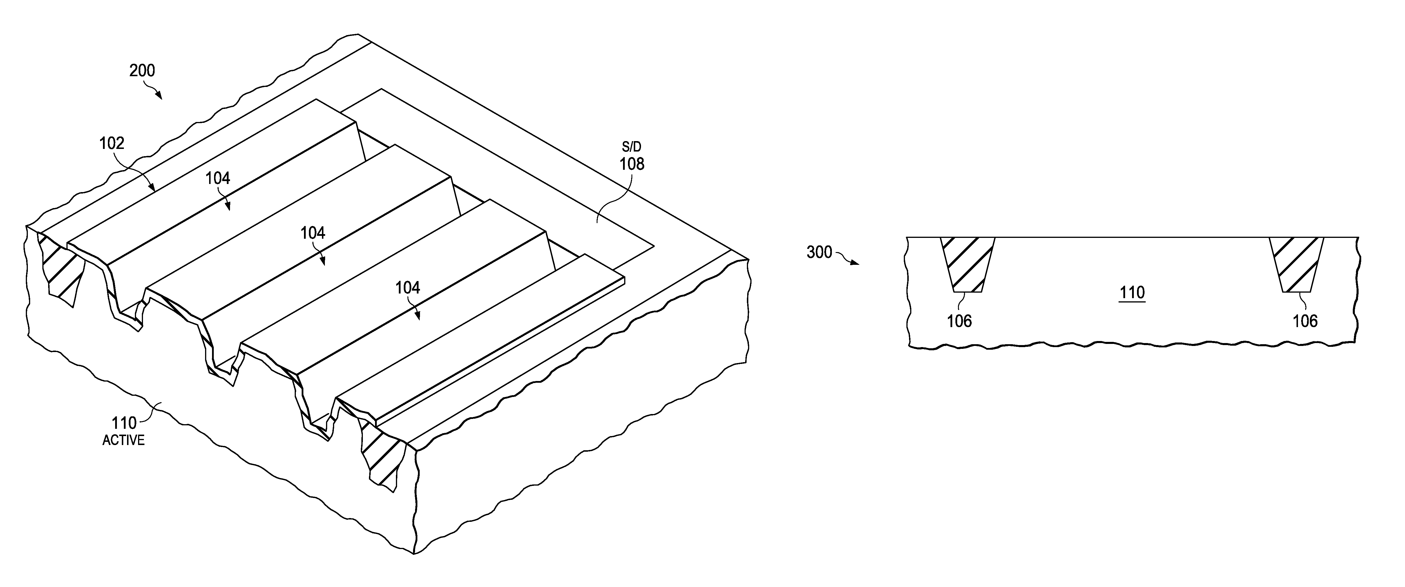
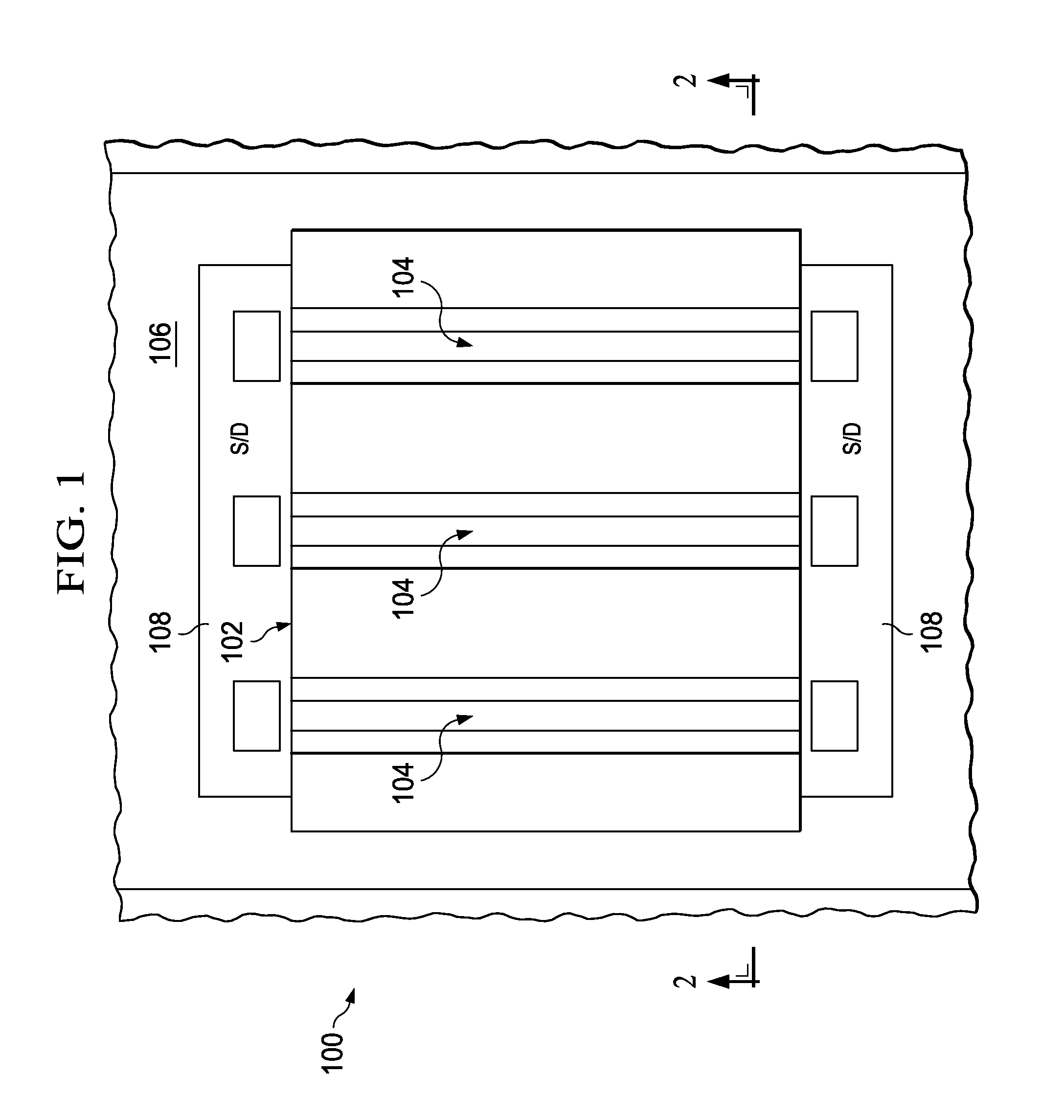
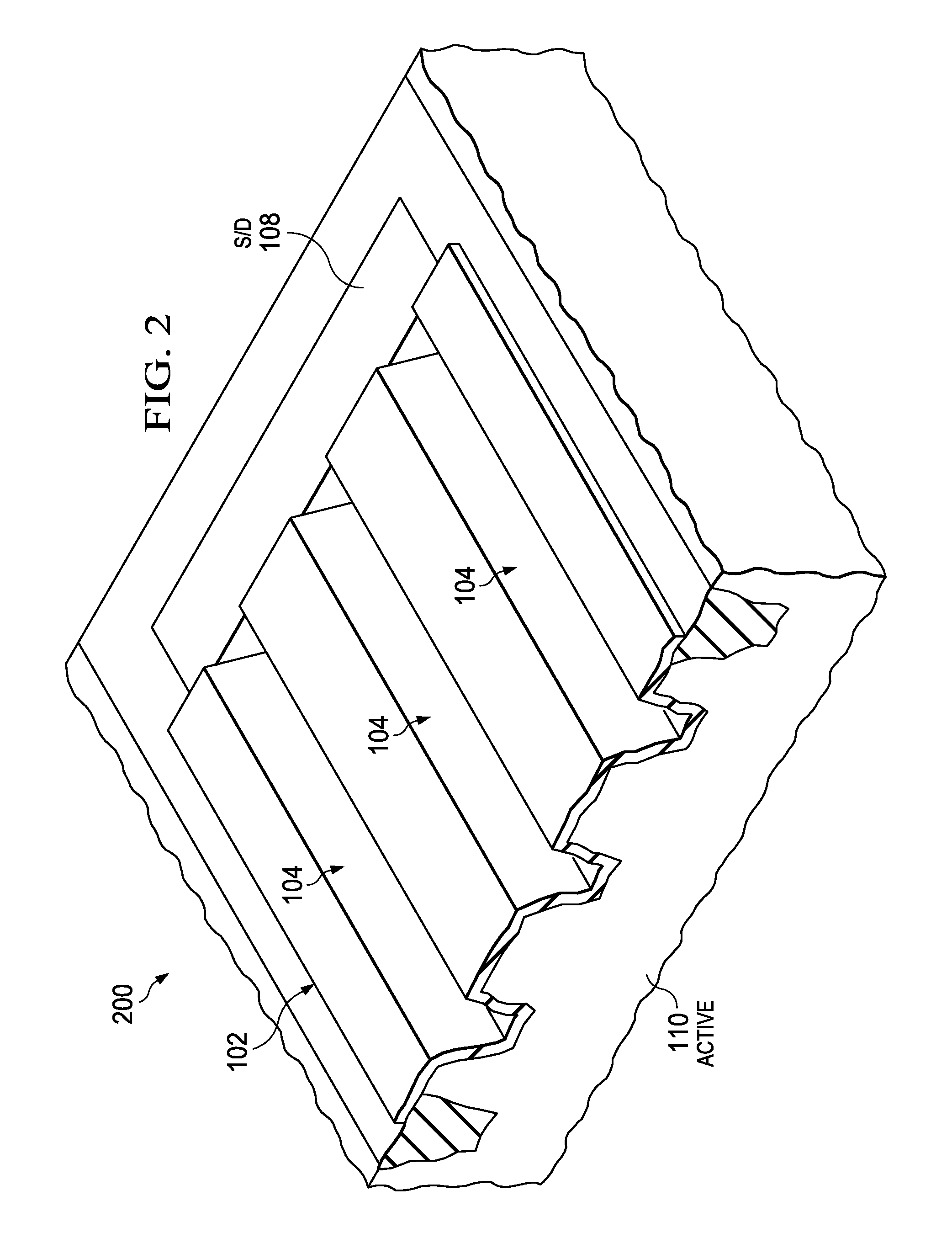
[0030]One or more implementations of the present invention will now be described with reference to the attached drawings, wherein the reference numerals are used to refer to like elements throughout, and wherein various structures are not necessarily drawn to scale. The method of the present invention will be described with reference to the formation of recessed active trenches for wide transistors. However, the method is applicable to other processes, for example, a process for forming any suitable digital or analog electronic device, for example, large switches, I / O devices, logic devices, analog devices, power IC outputs, switches, large inverter switches, and the like. Furthermore, while the following detailed description is presently contemplated by the inventors for practicing the invention, it should be understood that the description of this embodiment is merely illustrative and that it should not be taken in a limiting sense.

[0031]The present invention provides for a method...


PUM


Abstract

A method of manufacturing a semiconductor device having recessed active trenches by providing a substrate with STI and active regions, forming a first oxide layer on the substrate, forming an nitride layer on the first oxide layer, employing a photolithographic process to create at least one recessed active trench through the first oxide layer and the nitride layer and into the substrate to create an isolation region, wherein the at least one trench is perpendicular to at least one gate structure in an active area of the substrate, layering the trench with a second oxide layer, removing the first oxide layer and second oxide layer, forming a third oxide layer on the planar substrate with recessed active trench, and forming the at least one circuitous gate structure on the third oxide layer connecting at least one electronic source and drain.

Description

FIELD OF INVENTION[0001]The present invention relates generally to the fabrication of integrated circuits and more particularly to methods for creating recessed active trenches for wide transistors in order to increase the drive current (Ion) of the transistors, while the leakage current (Ioff) remains relatively constant.BACKGROUND OF THE INVENTION[0002]Integrated circuits are manufactured by fabricating electrical devices on semiconductor substrates and interconnecting the various electrical devices. Shallow trench isolation (STI) is a technique used to electrically isolate transistors or electrical devices and is a facilitating technology for the fabrication of advanced microelectronic devices, for example, complementary metal-oxide-semiconductors (CMOS). STI has largely replaced localized oxidation of silicon (LOCOS) isolation methods in the fabrication of advanced microelectronic devices. STI involves creating oxide isolation trenches for electrical separation or segregation in...

Claims


Application Information

Patent Timeline
Patent Type & Authority Patents(United States)
IPC IPC(8): H01L21/8234
CPCH01L21/76232H01L29/1037H01L29/42376H01L29/66621H01L29/78
Inventor MARSHALL, ANDREWBARNA, GABRIEL GEORGE
Owner TEXAS INSTR INC
Why Eureka
Try Eureka