Liquid crystal display device

a liquid crystal display and display panel technology, applied in non-linear optics, instruments, optics, etc., can solve the problems of affecting and affecting the quality of liquid crystal display devices. achieve the effect of improving the manufacturing yield of liquid crystal display devices

Active Publication Date: 2010-01-12
PANASONIC LIQUID CRYSTAL DISPLAY CO LTD +1
View PDF6 Cites 23 Cited by
  • Summary
  • Abstract
  • Description
  • Claims
  • Application Information

AI Technical Summary

Benefits of technology

[0015]The invention has been made to solve the problems of the related art, and the advantage of the invention is the ability to provide a technology by which the manufacturing yield of a liquid crystal display device can be increased.
[0016]These and other advantages and novel features of the invention will be apparent from the description in the specification and the accompanying drawings.
[0017]Representative aspects of the invention disclosed herein will be described as follows:
[0018](1) A liquid crystal display device includes a liquid crystal display panel and a resin-molded frame that houses the liquid crystal display panel, the liquid crystal display panel including a first substrate, a second substrate, and a liquid crystal layer sandwiched between the first and second substrates, the two-dimensional shapes of the first and second substrates being rectangles having longer sides and shorter sides, the longer side of the first substrate being longer than the longer side of the second substrate, the first substrate having a non-overlapping area that does not overlap with the second substrate, and among the four corners of the first substrate, the non-overlapping area of the first substrate having two corners adjacent to each other. At least one of the two corners forms a chamfered structure having a diagonal side that intersects the longer and shorter sides of the first substrate with the diagonal side inclined to the longer and shorter sides. At the corner of the chamfered structure, by drawing imaginary extensions of the longer and shorter sides of the first substrate and letting S be the intersection of the extended longer and shorter sides, P1 be the intersection of the shorter side and the diagonal side, P2 be the intersection of the longer side and the diagonal side, A be the distance from the point P1 to the point S, and B be the distance from the point P2 to the point S, the relationship A>B is satisfied.
[0019](2) In the description (1), the liquid crystal display panel has a plurality of subpixels, each of the plurality of subpixels having a pixel electrode and a counter electrode formed on the first substrate, and a conductive resin is applied onto the non-overlapping area of the first substrate.
[0020](3) A liquid crystal display device includes a liquid crystal display panel and a resin-molded frame that houses the liquid crystal display panel, the liquid crystal display panel including a first substrate, a second substrate, and a liquid crystal layer sandwiched between the first and second substrates, the two-dimensional shapes of the first and second substrates being rectangles having longer sides and shorter sides, the longer side of the first substrate being longer than the longer side of the second substrate, the first substrate having a non-overlapping area that does not overlap with the second substrate, and among the four corners of the first substrate, the non-overlapping area of the first substrate having two corners adjacent to each other. At least one of the two corners forms a chamfered structure having a diagonal side that intersects the longer and shorter sides of the first substrate with the diagonal side inclined to the longer and shorter sides. At the corner of the chamfered structure, by drawing imaginary extensions of the longer and shorter sides of the first substrate and letting S be the intersection of the extended longer and shorter sides, P1 be the intersection of the shorter side and the diagonal side, P2 be the intersection of the longer side and the diagonal side, A be the distance from the point P1 to the point S, and B be the distance from the point P2 to the point S, the relationship A<B is satisfied.

Problems solved by technology

In the liquid crystal display module having such a configuration, when the liquid crystal display panel is mounted in the recess of the resin-molded frame, there is concern that misalignment between the recess of the resin-molded frame and the liquid crystal display panel results in a problem, such as cracking and chipping, at the corners of the liquid crystal display panel.
Such problems frequently occur particularly when glass substrates are used as the two substrates (first and second substrates) that form the liquid crystal display panel.
Since the first substrate of the liquid crystal display panel has the non-overlapping area, such problems frequently occur at the corners of the non-overlapping area of the first substrate.
However, as described above, the presently used glass substrate with a thickness of 0.5 to 0.4 mm also has the problems, such as cracking and chipping, at corners of the liquid crystal display panel due to misalignment between the liquid crystal display panel and the recess of the resin-molded frame when the liquid crystal display panel is mounted in the recess of the resin-molded frame, even though a clearance is provided at each corner of the resin-molded frame.
In such circumstances, use of a glass substrate with a thickness of 0.3 mm or thinner reduces the mechanical strength of the substrate itself, so that there is concern over an increase in the risk of occurrence of the problems, such as cracking and chipping, at the corners of the liquid crystal display panel.
Such an increase leads to a reduced manufacturing yield of the liquid crystal display module.

Method used


Image

  • Liquid crystal display device
  • Liquid crystal display device
  • Liquid crystal display device

Examples


first embodiment

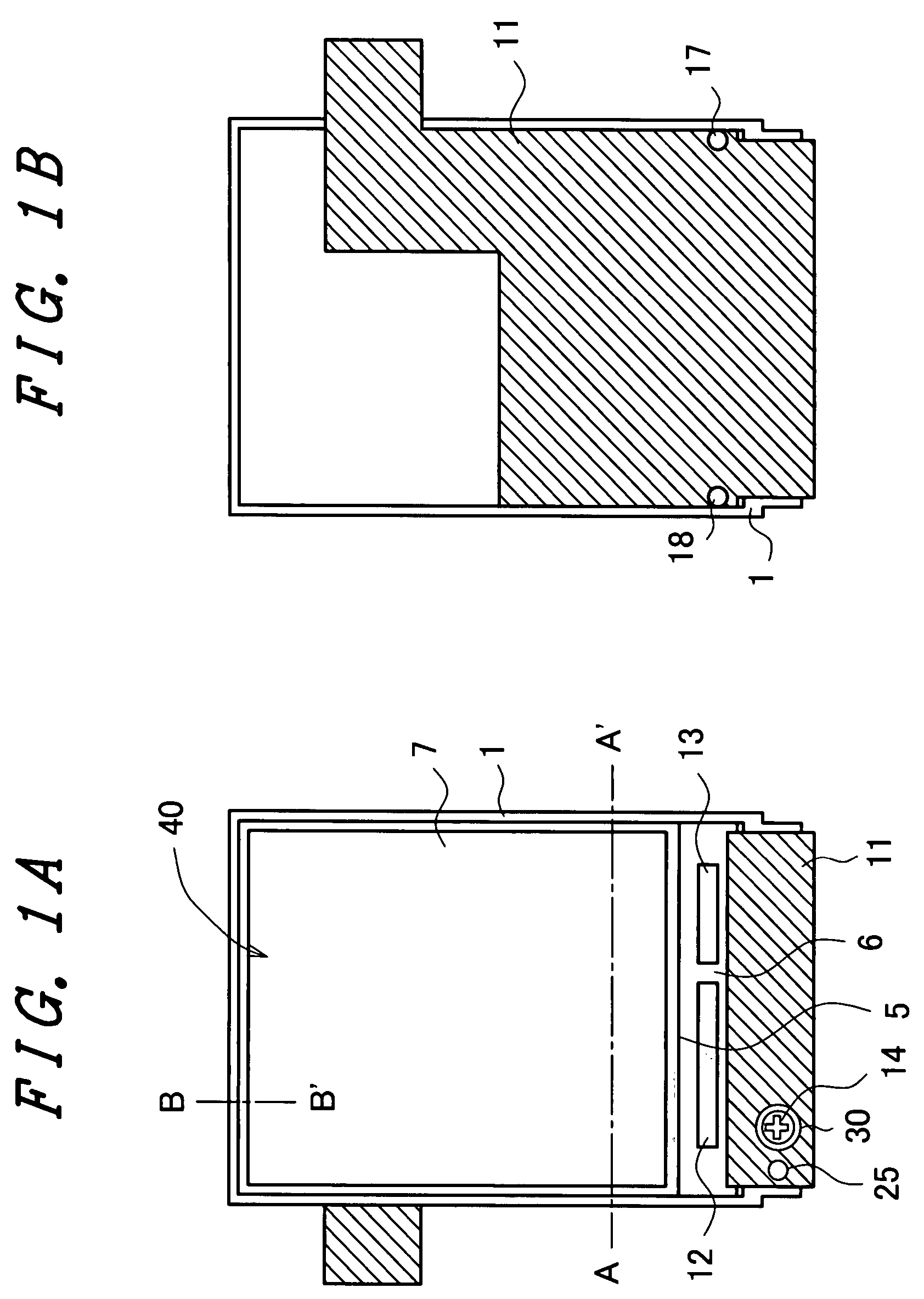
[0039]FIGS. 1A and 1B show a liquid crystal display module, which is a first embodiment of the invention. FIG. 1A is a top view (viewed from the liquid crystal display panel side, the front side or the observer side), and FIG. 1B is a bottom view (viewed from the light guide plate side, the rear side or the back side).

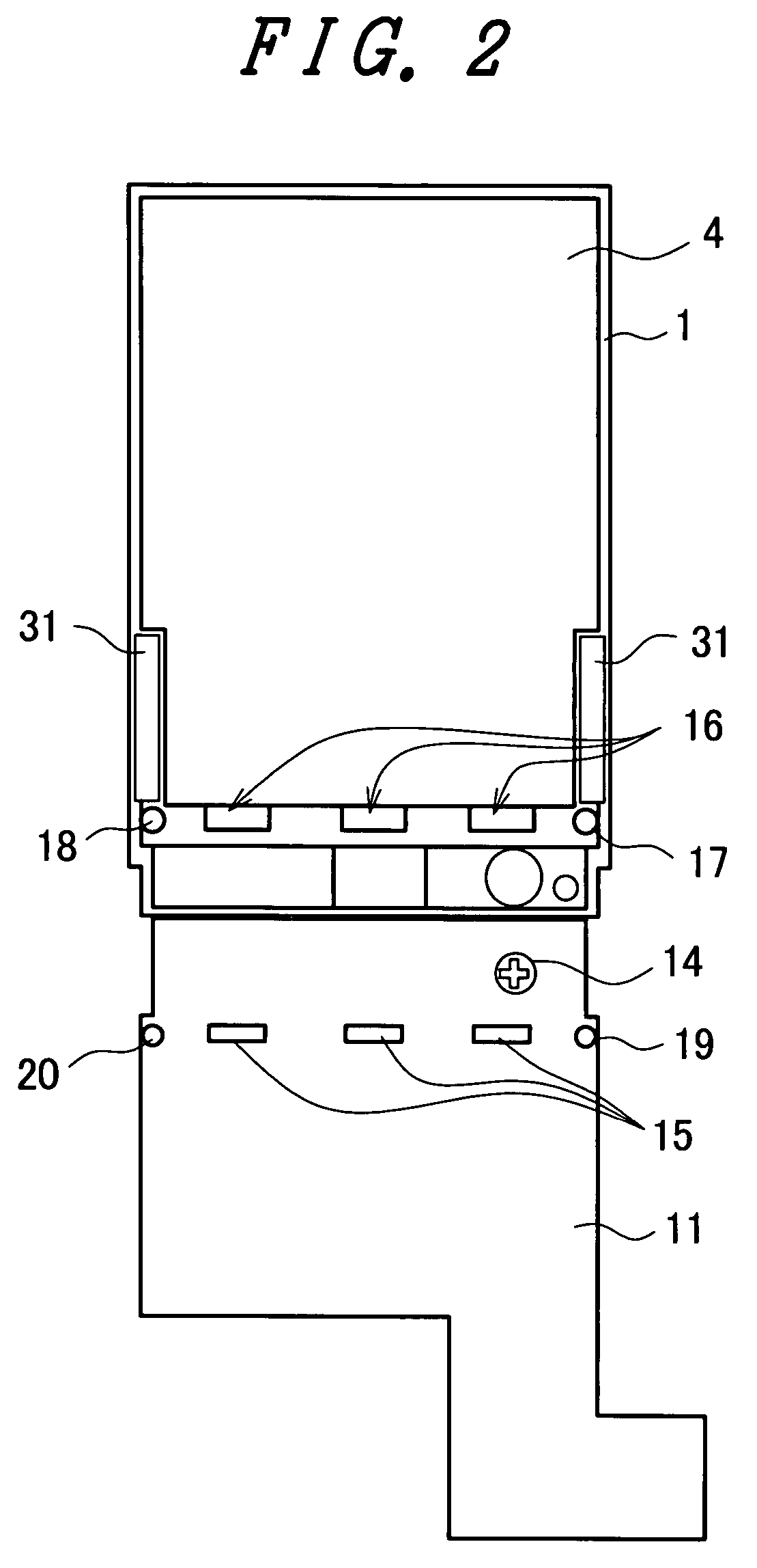
[0040]FIG. 2 shows the liquid crystal display module in FIG. 1B with a flexible printed circuit board (FPC) 11 unfolded.

[0041]Reference numerals in these figures denote the following portions. Reference numeral 1 denotes a resin-molded frame (resin-molded body). Reference numeral 4 denotes a reflective sheet. Reference numerals 5 and 6 denote glass substrates. Reference numeral 7 denotes an upper polarizer. Reference numeral 11 denotes a flexible printed circuit board (FPC). Reference numerals 12 and 13 denote semiconductor chips on which driver circuits are mounted. Reference numeral 14 denotes a pre-set resistance element for adjusting Vcom. Reference numeral 15 deno...

second embodiment

[0070]FIG. 9 shows part of a liquid crystal display panel in a liquid crystal display module, which is a second embodiment of the invention.

[0071]The liquid crystal display module according to the second embodiment basically has a configuration similar to that of the first embodiment described above except for the following points.

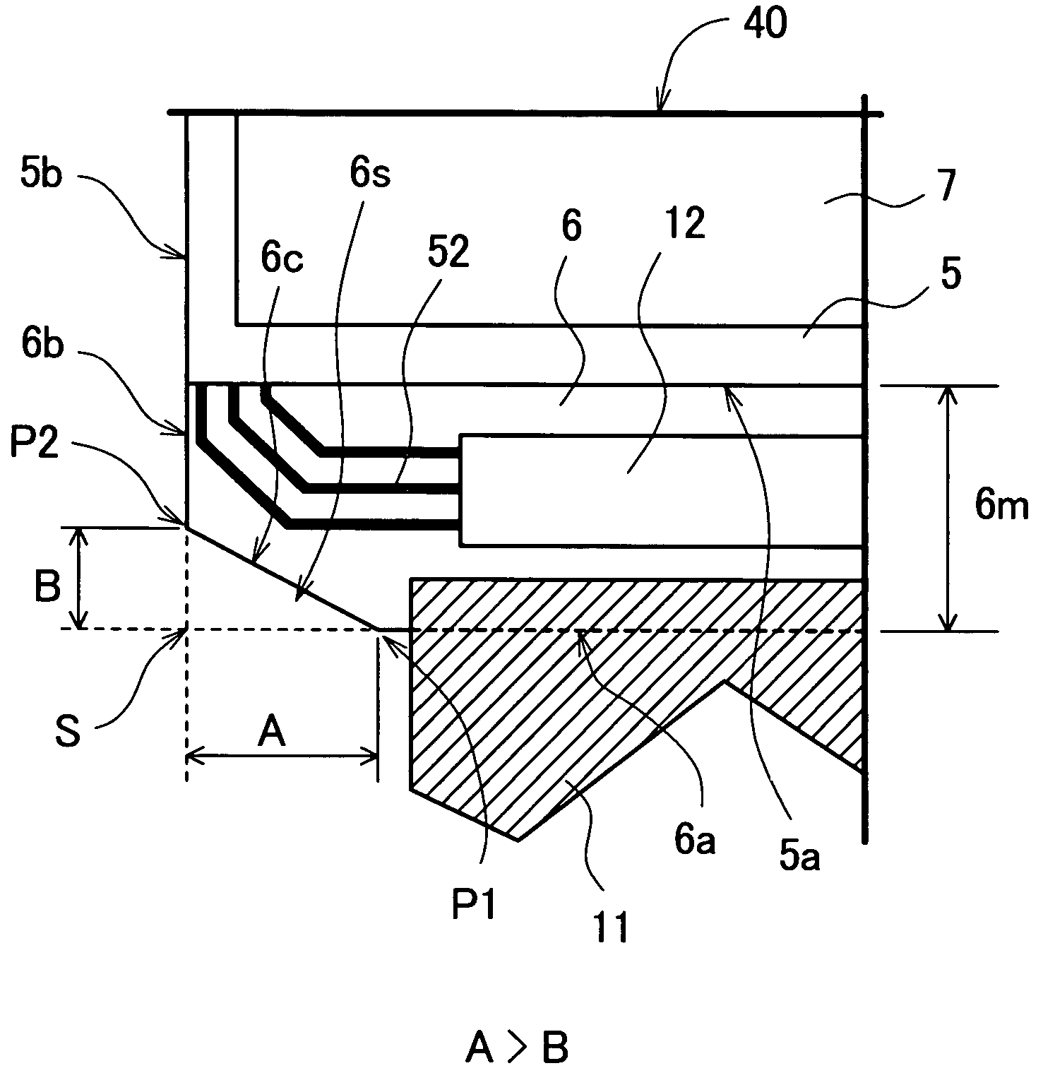
[0072]That is, in the first embodiment, as shown in FIG. 7, the corners 6s of the chamfered structures (two corners in the non-overlapping area 6m of the glass substrate 6) satisfy the relationship A>B, while in the second embodiment, as shown in FIG. 9, the corners 6s of the chamfered structures (two corners in the non-overlapping area 6m of the glass substrate 6) satisfy the relationship A

[0073]In such a configuration, when the liquid crystal display panel is mounted in the recess of the resin-molded frame, the risk of occurrence of the problems, such as cracking and chipping, at the corners of the liquid crystal display panel (corners 6s of the non-o...


PUM

PropertyMeasurementUnit
thicknessaaaaaaaaaa
thicknessaaaaaaaaaa
widthaaaaaaaaaa

Abstract

The liquid crystal display (LCD) device of the present invention includes a LCD panel and a resin-molded frame that houses the LCD panel, the LCD panel including first and second substrates, and a liquid crystal layer sandwiched between the first and second substrates. The two-dimensional shapes of the first and second substrates are rectangles having longer and shorter sides, the longer side of the first substrate being longer than that of the second substrate. The first substrate has a non-overlapping area that does not overlap with the second substrate. Among the four corners of the first substrate, the non-overlapping area of the first substrate has two corners adjacent to each other. At least one of the two corners forms a chamfered structure having a diagonal side that intersects the longer and shorter sides of the first substrate with the diagonal side inclined to the longer and shorter sides.

Description

[0001]The present application claims priority from Japanese application JP2006-249009 filed on Sep. 14, 2006, the content of which is hereby incorporated by reference into this application.BACKGROUND OF THE INVENTION[0002]The present invention relates to a liquid crystal display device, and particularly to a technology that is effective when applied to a liquid crystal display device in which a liquid crystal display panel is mounted in a resin-molded frame.[0003]ATFT (Thin Film Transistor) liquid crystal display module having a small-size liquid crystal display panel with approximately 240×320×3 subpixels in a color display mode is widely used as the display section of a mobile apparatus, such as a mobile phone.[0004]The liquid crystal display module used as the display section of a mobile apparatus, such as a mobile phone, includes a liquid crystal display panel and a resin-molded frame that houses the liquid crystal display panel, and the liquid crystal display panel is housed in...

Claims


Application Information

Patent Timeline
Patent Type & Authority Patents(United States)
IPC IPC(8): G02F1/1333
CPCG02F1/1333G02F1/133308G02F1/13452G02F2001/133302G02F2001/133317G02F2001/133322G02F2001/133334G02F1/133302G02F1/133317G02F1/133322G02F1/133334
Inventor HASHIMOTO, SHINYA
Owner PANASONIC LIQUID CRYSTAL DISPLAY CO LTD
Why Eureka
Try Eureka