
Ceramic coating member for semiconductor processing apparatus

a technology of ceramic coating and processing apparatus, which is applied in the direction of magnetic materials, energy-based chemical/physical/physico-chemical processes, railway signalling, etc., can solve the problems of destroying devices, insufficient conventional method of coating with oxide of elements of group iiib, etc., and achieves improved corrosion resistance of substrates, high energy, and high energy.

Active Publication Date: 2010-01-19
TOCALO CO LTD +1
View PDF144 Cites 36 Cited by
  • Summary
  • Abstract
  • Description
  • Claims
  • Application Information

AI Technical Summary

Benefits of technology

[0057]Of course, these conditions are not limited to the above ranges as far as the predetermined effects of the invention are obtained.
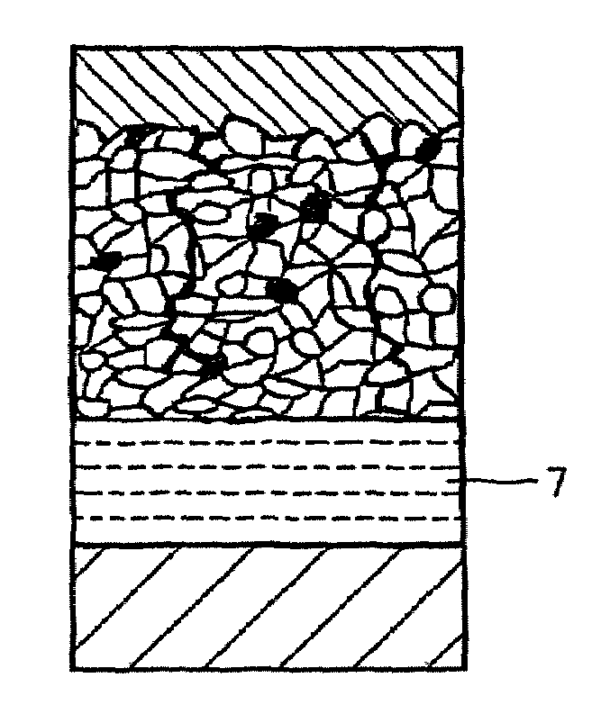
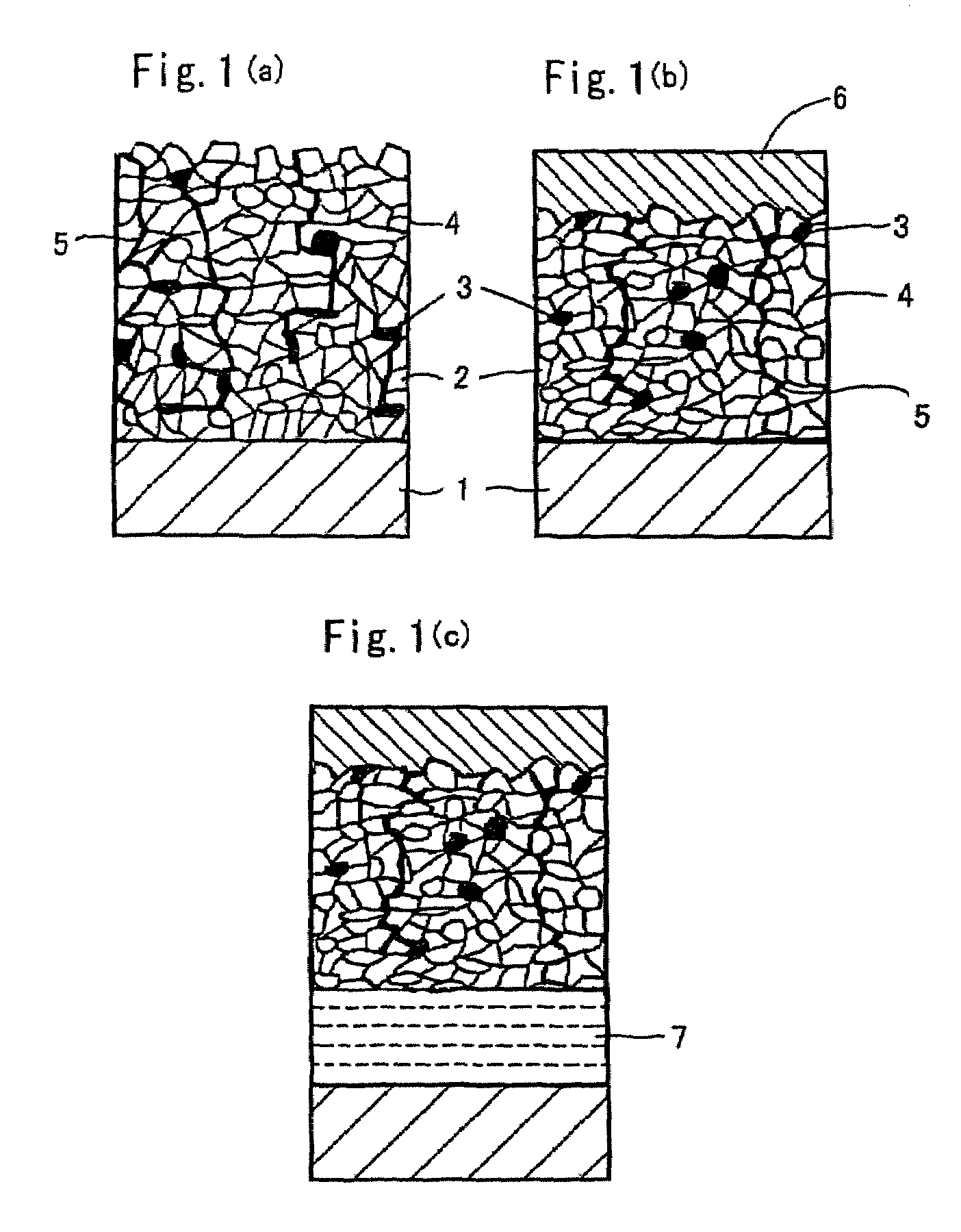
[0058]The oxide of the Group IIIb element subjected to the electron beam irradiation treatment has its temperature rising from the surface and finally reaches above its melting point to become a fused state. Such a fusion phenomenon gradually comes into the interior of the coating as the irradiation output of the electron beam becomes high or the irradiation frequency increases or the irradiation time becomes long, so that the depth of the irradiation-fused layer can be controlled by changing the irradiation conditions. When the fusion depth is 100 μm or less, practically 1-50 μm, the secondary recrystallized layer achieving the above objectives is obtained.
[0059](2) Laser beam irradiation treatment: It is possible to use YAG laser utilizing YAG crystal or CO2 gas laser using a gas as a medium, or the like. In the laser beam irradiation treatment the following conditions are recommended:
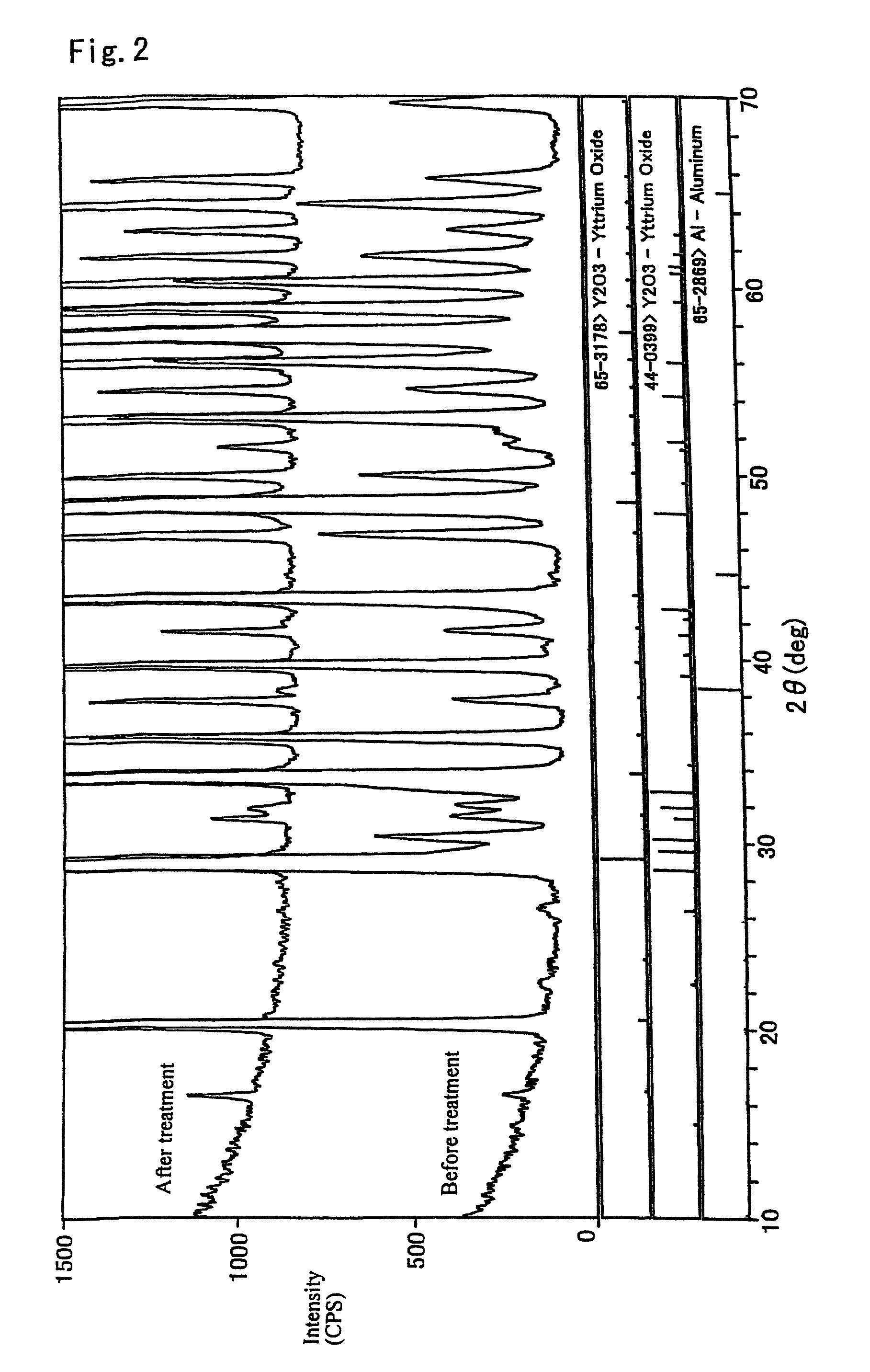
[0063]As mentioned above, the layer subjected to the above electron beam irradiation treatment or laser beam irradiation treatment is changed into a physically and chemically stable crystal form by transforming at a high temperature and precipitating secondary recrystals in the cooling, so that the modification of the coating proceeds in a unit of crystal level. For example, the Y2O3 coating formed by the atmospheric plasma spraying method is a mixed crystal including the rhombic crystal at the sprayed state as previously mentioned, while it changes into substantially a cubic crystal after the electron beam irradiation.
[0064]The features of the secondary recrystallized layer made from the oxide of the Group IIIb element subjected to the high energy irradiation treatment are summarized as follows.
[0065]a) The secondary recrystallized layer produced by the high energy irradiation treatment being formed by further secondary-transforming the porous layer made of the metal oxide or the like as an underlayer primary transformed layer, or with the oxide particles of the underlayer being heated at above the melting point, is densified by disappearance of at least a part of pores.

Problems solved by technology

However, the conventional method of covering with the oxide of the element of Group IIIb is not yet sufficient in the recent semiconductor processing technique requiring high precision processing and environmental cleanness in a further severer corrosive gas atmosphere.
Moreover, particles as a corrosion product are produced in such an environment, which drop down and adhere onto a surface of an integrated circuit in the semiconductor product to result in a cause of damaging the device.

Method used


Image

  • Ceramic coating member for semiconductor processing apparatus
  • Ceramic coating member for semiconductor processing apparatus
  • Ceramic coating member for semiconductor processing apparatus

Examples


example 1

[0084]In this example, an undercoat (spray coating) of 80 mass % Ni-20 mass % Cr is formed on a surface of an Al substrate (size: 50 mm×50 mm×5 mm) by an atmospheric plasma spraying method and a porous coating is formed thereon with powders of Y2O3 and CeO2 by the atmospheric plasma spraying method, respectively. Thereafter, the surfaces of the spray coating are subjected to two kinds of high energy irradiation treatments, i.e. electron beam irradiation and laser beam irradiation. Then, the surface of the thus obtained coating to be tested is subjected to a plasma etching work under the following conditions. The number of particles of coating element scraped and flying from the coating through the etching treatment is measured to examine the resistance to plasma erosion and the resistance to environmental contamination. The comparison is conducted by measuring a time that 30 particles having a particle size of 0.2 μm or more adhere to the surface of a silicon wafer of 8 inches in di...

example 2

[0104]In this example, a coating is formed by spraying a film-forming material as shown in Table 3 onto a surface of an Al substrate having a size of 50 mm×100 m×5 mm. Thereafter, a part of the coating is subjected to an electron beam irradiation treatment for forming a secondary recrystallized layer suitable for the invention. Then, a specimen having a size of 20 mm×20 mm×5 mm is cut out from the resulting treated coating and is masked so as to expose an area of 10 mm×10 mm, which is subjected to a plasma irradiation under the following conditions, and thereafter an amount damaged through plasma erosion is measured by means of an electron microscope or the like.[0105](1) Gas atmosphere and flowing condition[0106]CF4 / Ar / O2=100 / 1000 / 10 ml (flow amount per 1 minute)[0107](2) Plasma irradiation output[0108]High frequency power: 1300 W[0109]Pressure: 133.3 Pa

[0110]The above results are summarized in Table 3. As seen from the results of this table, all of the anodized coating (No. 8), B4...

example 3

[0117]In this example, the resistance to plasma erosion in the coating formed by the method of Example 2 before and after the electron beam irradiation treatment is examined. As a specimen to be tested, ones obtained by directly forming the following mixed oxide onto an Al substrate at a thickness of 200 μm through an atmospheric plasma spraying method are used.[0118](1) 95% Y2O3-5% SC2O3 [0119](2) 90% Y2O3-10% Ce2O3 [0120](3) 90% Y2O3-10% Eu2O3

[0121]Moreover, the electron beam irradiation and gas atmosphere element after the film formation, plasma irradiation conditions and the like are the same as in Example 2.

[0122]The above results are summarized in Table 4 as an amount damaged through plasma erosion. As seen from the results of this table, the coatings of oxides in Group IIIb of the Periodic Table under the conditions adaptable for the invention are better in the resistance to plasma erosion even in the use at the mixed oxide state as compared with the Al2O3 (anodizing) and B4...


PUM

PropertyMeasurementUnit
porosityaaaaaaaaaa
thicknessaaaaaaaaaa
porosityaaaaaaaaaa

Abstract

Improving the resistance of members and parts disposed inside of vessels such as semiconductor processing devices for conducting plasma etching treatment in a strong corrosive environment. A ceramic coating member for a semiconductor processing apparatus comprises a porous layer made of an oxide of an element in Group IIIb of the Periodic Table coated directed or through an undercoat on the surface of the substrate of a metal or non-metal and a secondary recrystallized layer of the oxide formed on the porous layer through an irradiation treatment of a high energy such as electron beam and laser beam.

Description

FIELD OF THE INVENTION[0001]This invention relates to a ceramic coating member for a semiconductor processing apparatus, which is more particularly used as a coating member for members, parts and the like disposed in a semiconductor treating vessel for conducting a plasma etching process or the like.BACKGROUND OF THE INVENTION[0002]In devices used in the field of semiconductor or liquid crystal, they are frequently processed by using plasma energy of a halogen-based corrosive gas having a high corrosion property. For example, the fine wiring pattern to be formed by the semiconductor processing device is formed by fine processing (etching) utilizing a strong reactivity of ion or electron excited when a plasma is generated in a strongly corrosive gas atmosphere of a fluorine or chlorine or a mixed gas atmosphere with an inert gas thereof.[0003]In case of such a processing technique, the members or parts (susceptor, electrostatic chuck, electrode and others) disposed in at least a part...

Claims


Application Information

Patent Timeline
Patent Type & Authority Patents(United States)
IPC IPC(8): H01L29/04B01J19/08B01J3/08B05D1/06B05D3/06C01F17/00C04B35/505C08J7/18C23C4/10H01L21/3105H01L21/461H01L21/473
CPCC23C4/02C23C28/042C23C4/18Y10T428/12
Inventor KOBAYASHI, YOSHIYUKIMURAKAMI, TAKAHIROHARADA, YOSHIOTAKEUCHI, JUNICHIYAMASAKI, RYOKOBAYASHI, KEIGO
Owner TOCALO CO LTD
Learn More