Semiconductor memory device, test circuit and test method

a memory device and semiconductor technology, applied in the field of semiconductor memory devices, can solve the problems of increasing test costs, unable to ensure the correctness of device quality, and unable to ensure so as to reduce the time and cost of testing and improve the quality of the devi

Active Publication Date: 2010-01-26
RENESAS ELECTRONICS CORP
View PDF14 Cites 5 Cited by
  • Summary
  • Abstract
  • Description
  • Claims
  • Application Information

AI Technical Summary

Benefits of technology

[0034]In short, it is not that easy to carry out testing of, for example, the interference between the read / write operation and the refresh, as the read / write operation and the refresh are set to the state of closest proximity to each other. If an attempt is made to conduct the testing, the result is an increased test cost, as described above.
[0040]According to the present invention, setting may be made for compulsorily generating the refresh in the worst timing state, during testing, for thereby reducing the time and cost for testing and improving the quality of the device.

Problems solved by technology

Due to this randomness, overmuch time is taken in testing for checking the interference between the read / write operation and the refresh operation, with the result that the test cost is increased, while the quality of the device can hardly be assured.
However, if the refresh request and the read / write request do not temporally collide one on the other, the probable state of closest proximity of the read / write request to the refresh request cannot be confirmed, as a result of which the quality of the device cannot be assured correctly.
In short, it is not that easy to carry out testing of, for example, the interference between the read / write operation and the refresh, as the read / write operation and the refresh are set to the state of closest proximity to each other.
If an attempt is made to conduct the testing, the result is an increased test cost, as described above.

Method used


Image

  • Semiconductor memory device, test circuit and test method
  • Semiconductor memory device, test circuit and test method
  • Semiconductor memory device, test circuit and test method

Examples


Embodiment Construction

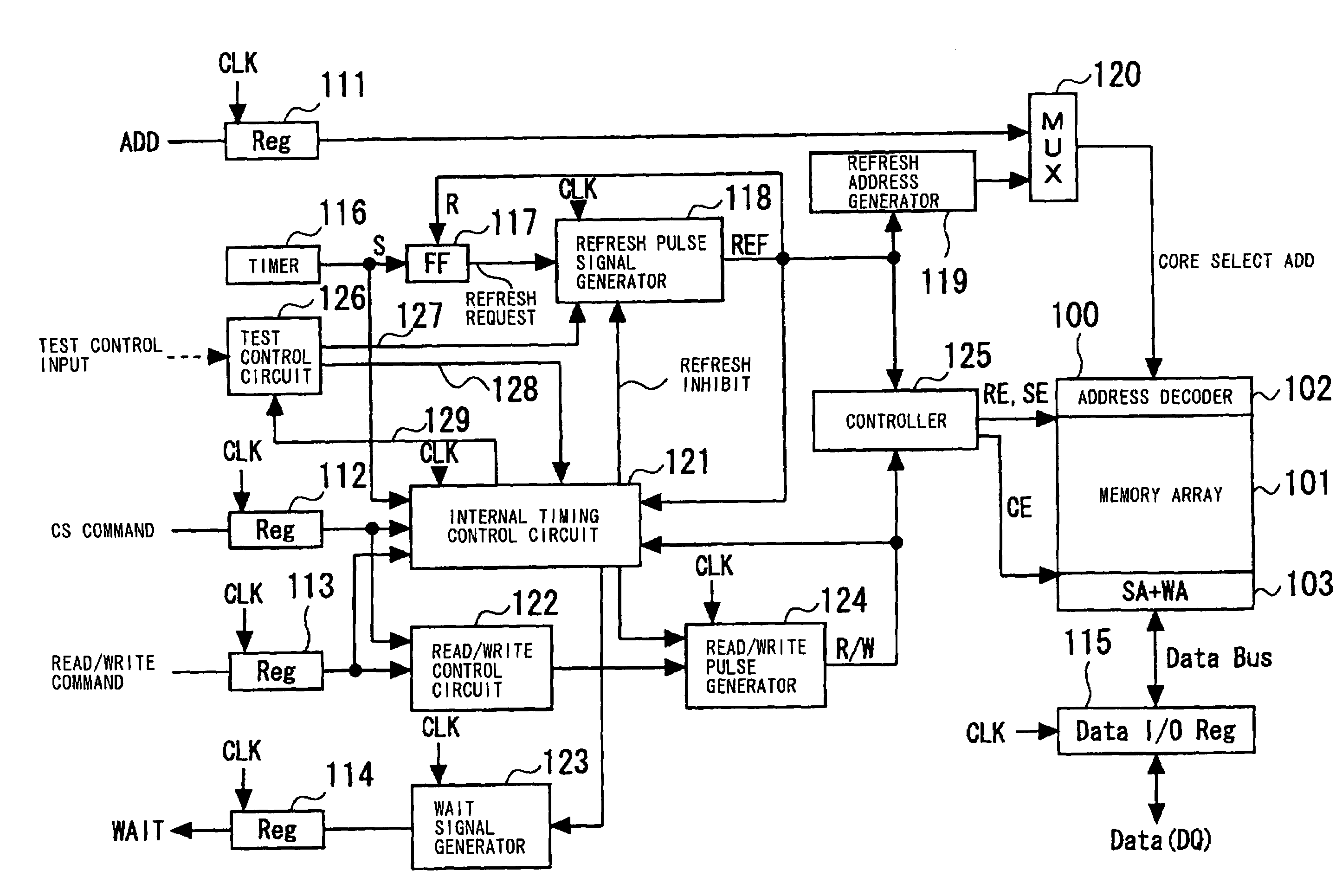
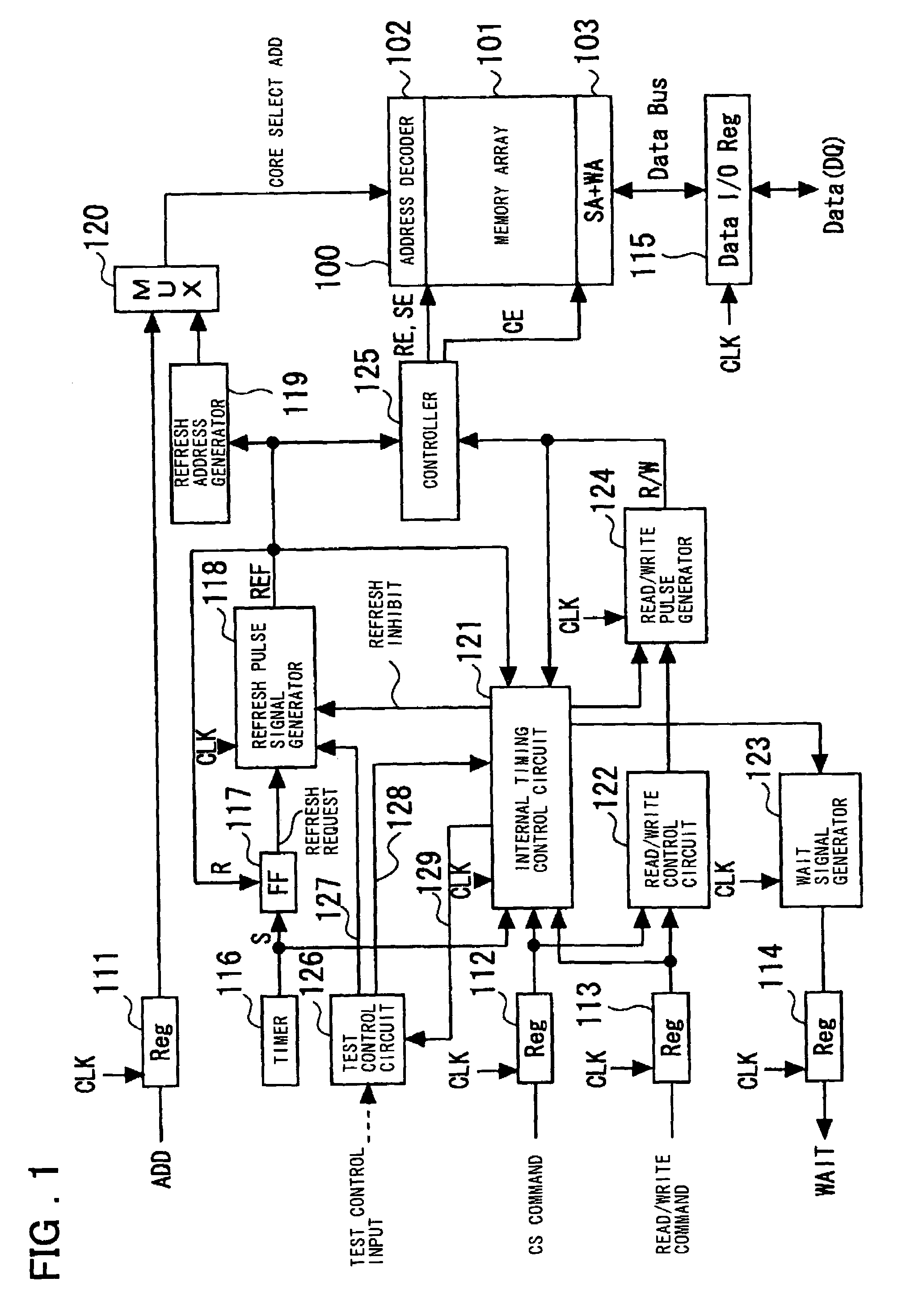
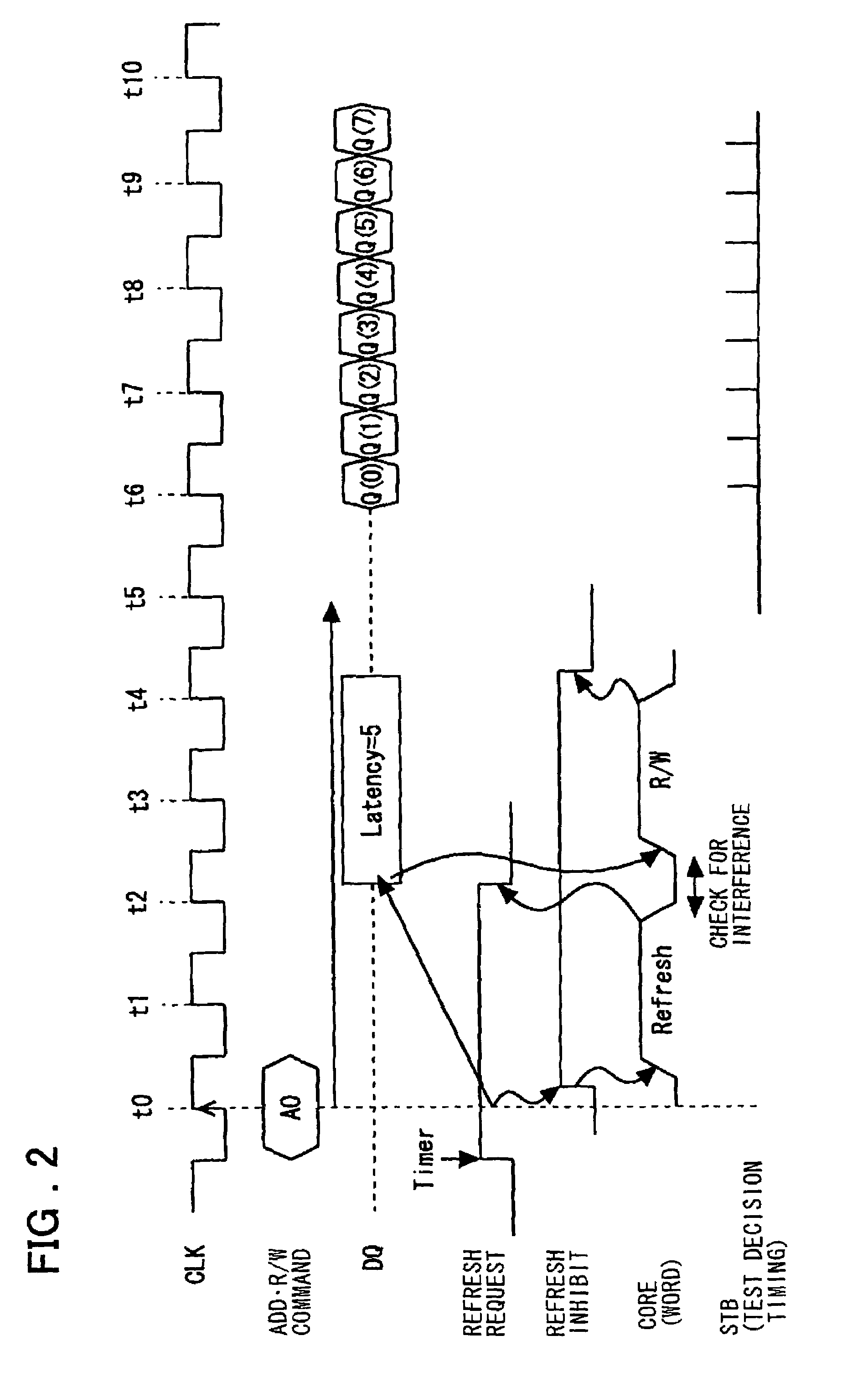
[0048]For elucidating the present invention in further detail, reference is made to the accompanying drawings. In an embodiment of the present invention, the relationship between the temporally forward state and the temporally backward state of the read / write and the refresh is prepared at the time of testing, in connection with the temporally preceding or succeeding states of the read / write and the refresh, such that the state of closest proximity of refresh→read / write (mode 1) and the state of closest proximity of read / write→refresh (mode 2) can be generated intentionally.

[0049]That is, in the mode 1, refresh is necessarily generated immediately before the read / write operation, and the latency is fixed at all times at a constant value, such as at 5. In the mode 2, refresh is necessarily generated immediately after the read / write operation, and the latency is fixed at all times at a constant value, such as at 3. In the mode 1, the read / write is fixedly generated immediately after t...


PUM


Abstract

Disclosed is a semiconductor memory device having memory cells that are in need of refresh for data retention, includes control circuits for necessarily generating the refresh immediately before the read / write operation, and for setting the latency to a first fixed value at all times, for the first mode during the testing, and for necessarily generating the refresh immediately after the read / write operation, and for setting the latency to a second fixed value at all times, for the second mode during the testing.

Description

FIELD OF THE INVENTION[0001]This invention relates to a semiconductor memory device. More particularly, it relates to a semiconductor memory device, having memory cells in need of refresh for data retention, in which the access speed by refresh may be prevented from being lowered, and to a test method.BACKGROUND OF THE INVENTION[0002]The following analyses are given by the present invention.[0003]Such a semiconductor memory device that comprises a cell array formed by dynamic type memory cells in need of refresh for data retention, and that is adapted to operate as a static random access memory (SRAM), has so far been in use. This type of the semiconductor memory is also termed a pseudo SRAM or a pseudostatic DRAM. There have also been developed a RAM family (termed for example MSRAM) for use of a mobile application, which is functionally compatible with the low power SRAM and which has achieved a high storage capacity by exploiting DRAM memory cells (see Non-Patent Document 1, indi...

Claims


Application Information

Patent Timeline
Patent Type & Authority Patents(United States)
IPC IPC(8): G11C7/00
CPCG11C11/406G11C29/12015G11C29/14G11C11/401G11C2211/4061
Inventor TAKAHASHI, HIROYUKINAKAGAWA, ATSUSHIKERA, TAKUYAMIYATA, MASAKIKAWAGUCHI, YASUNARIGOTOU, KOUICHI
Owner RENESAS ELECTRONICS CORP
Why Eureka
Try Eureka