Fabrication method of semiconductor integrated circuit device

a technology of integrated circuit devices and fabrication methods, which is applied in the direction of semiconductor/solid-state device testing/measurement, semiconductor/solid-state device details, instruments, etc., can solve problems such as unsolved problems, reduced throughput, and reduced test efficiency, so as to reduce the cost of testing semiconductor integrated circuit devices, shorten the time required for testing, and low cost

Inactive Publication Date: 2007-12-11
RENESAS ELECTRONICS CORP
View PDF9 Cites 4 Cited by
  • Summary
  • Abstract
  • Description
  • Claims
  • Application Information

AI Technical Summary

Benefits of technology

[0010]The SiP is expected to significantly grow in demand in the future. To enhance the manufacturing efficiency, consideration has been given to shortening the time required for testing the semiconductor memory portion. The result of such consideration indicates that omission of burn-in and a shortening of the memory test time can be expected.
[0012]By preparing a large number of test boards for testing semiconductor integrated circuit devices, the influence of the time required for attaching and detaching semiconductor integrated circuit devices and the setup can be reduced. However, a problem is left unsolved. The test boards are densely mounted with sockets into which semiconductor integrated circuit devices are inserted and peripheral circuits, including FPGAs (Field Programmable Gate Arrays), SRAMs (Static Random Access Memories), buffers, and the like. Preparing a large number of test boards can extraordinarily increase the test cost.
[0014]An object of the present invention is to shorten the time required for testing semiconductor integrated circuit devices.
[0015]Another object of the present invention is to significantly reduce the cost of testing semiconductor integrated circuit devices.
[0017]A still further object of the present invention is to provide a test technique which makes it possible to carry out memory tests on semiconductor integrated circuit devices, including a semiconductor memory, at low cost with the efficiency.
[0034]With respect to a plurality of devices on a plurality of boards to be tested, loading to test equipment, the starting and ending of testing, and unloading from test equipment can be carried out on a board-by-board basis. As a result, the test cost can be reduced.

Problems solved by technology

However, there still remains a problem even though the test time can be shortened.
In batch processing, the throughput can be hardly enhanced because of the influence of the time required for attaching and detaching semiconductor integrated circuit devices and the setup.
However, a problem is left unsolved.
Preparing a large number of test boards can extraordinarily increase the test cost.

Method used


Image

  • Fabrication method of semiconductor integrated circuit device
  • Fabrication method of semiconductor integrated circuit device
  • Fabrication method of semiconductor integrated circuit device

Examples


Embodiment Construction

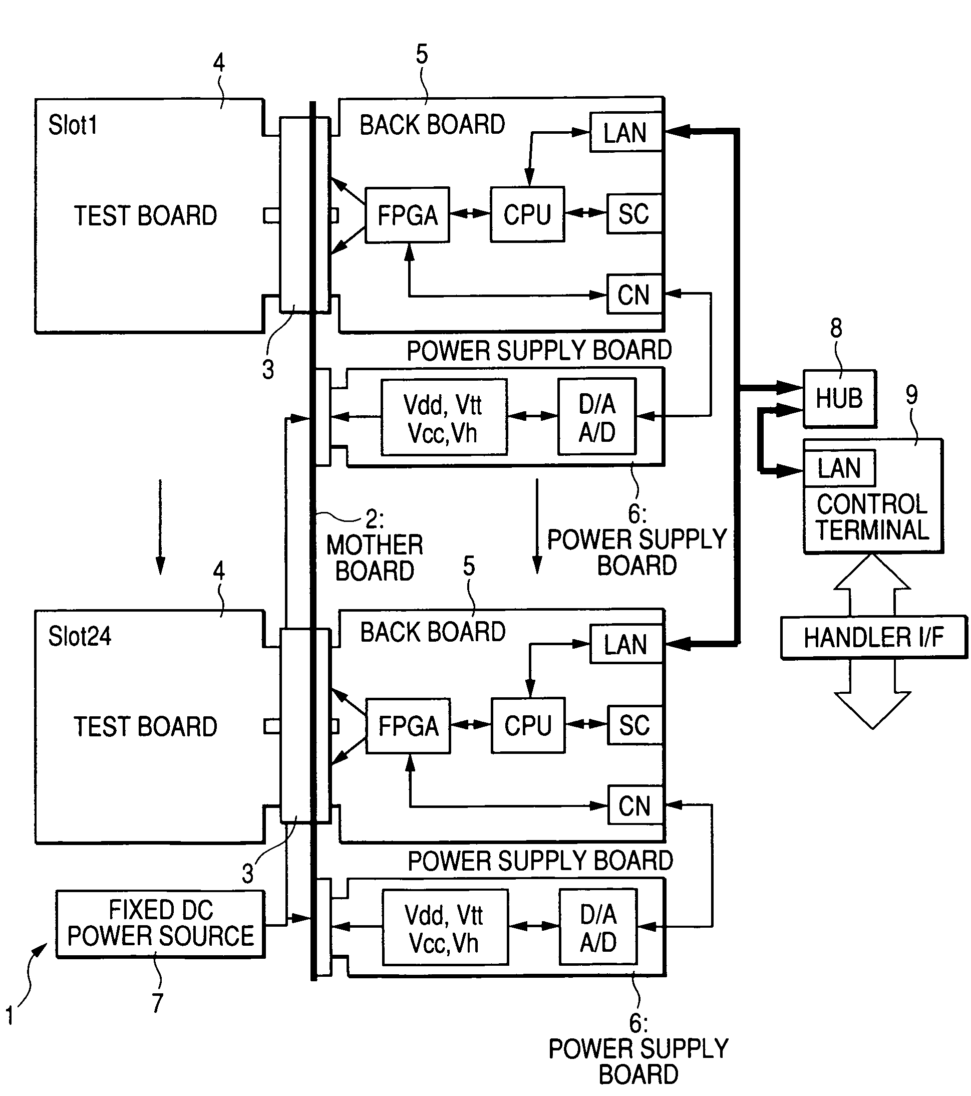
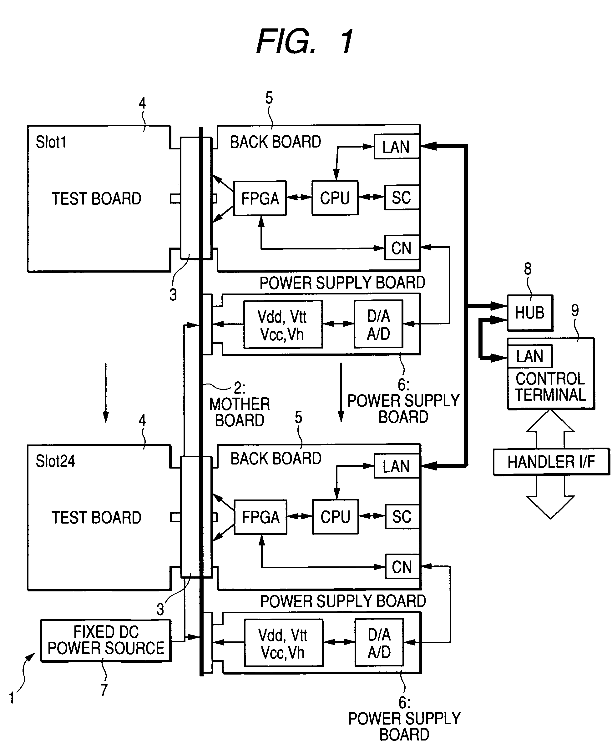
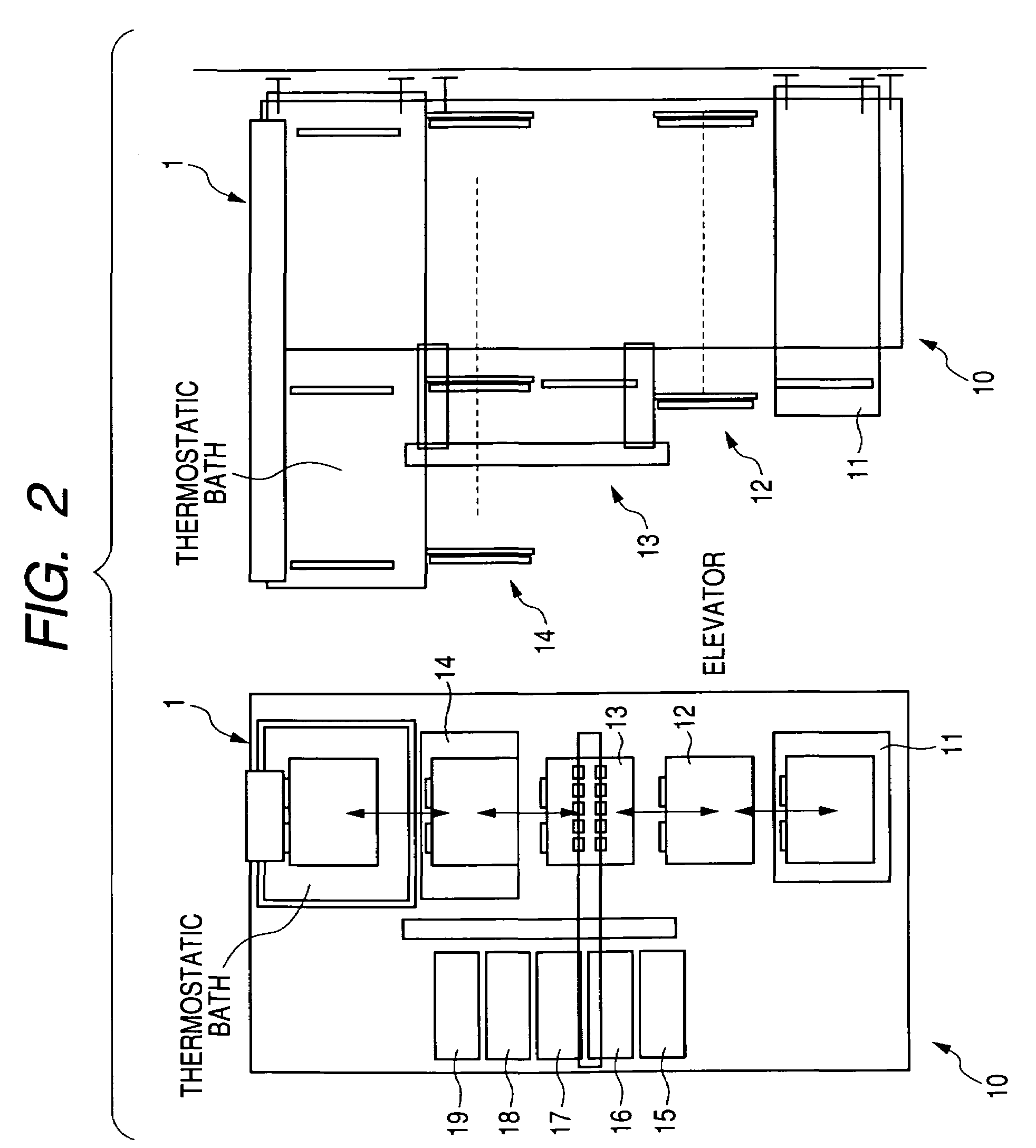
[0060]Embodiments of the present invention will be described in detail with reference to the drawings. In all of the drawings, the same members will be identified with the same numerals as a rule, and a repetitive description thereof will be omitted.

[0061]In the following description of the embodiments, the description of the same or similar elements will not be repeated as a rule unless especially needed.

[0062]In the following description of the present invention, the subject matter will be divided into a plurality of sections or embodiments if necessary for the sake of convenience. However, they are not unrelated to each other, but are in such a relation that one represents a modification to, the details of, the supplementary explanation of, or the like of part or all of the other unless otherwise stated.

[0063]If reference is made to any number of elements or the like (including a number of pieces, a numeric value, a range, and the like) in the description of the embodiments, the ...


PUM


Abstract

A memory test is carried out on semiconductor integrated circuit devices including a semiconductor memory at low cost with efficiency. In a test burn-in system, twenty-four test boards are processed in sequence with time differences, and the test boards are circulated one by one. In this case, the memory test is conducted with the sequence of single board processing: the test is started with a test board in which semiconductor integrated circuit devices have been embedded, and semiconductor integrated circuit devices are discharged, beginning with a test board that has undergone the test.

Description

CROSS-REFERENCE TO RELATED APPLICATION[0001]The present application claims priority from Japanese patent application No. 2003-425616, filed on Dec. 19, 2003, the content of which is hereby incorporated by reference into this application.BACKGROUND OF THE INVENTION[0002]The present invention relates to a method fabrication of semiconductor integrated circuit devices, and, more particularly, to a technique that is effective when applied to the testing of semiconductor integrated circuit devices, including semiconductor memories.[0003]Various techniques have been proposed with respect to test burn-in systems which evaluate and determine the acceptability of semiconductor integrated circuit devices that constitute devices to be tested in burn-in. An example of such proposals is Japanese Unexamined Patent Publication No. Hei 06(1994)-283657 (Patent Document 1). As described in Patent Document 1, test burn-in systems are based on batch processing.[0004]There are various test techniques fo...

Claims


Application Information

Patent Timeline
Patent Type & Authority Patents(United States)
IPC IPC(8): G01R31/26G01R31/28G11C29/56H01L21/66
CPCG01R31/286G11C29/56G11C29/56016G01R31/287H01L2224/16225G01R31/31718G11C2029/5602H01L2224/16227H01L2224/48227H01L2224/48247H01L2225/06558H01L2924/15311H01L2924/3025H01L2924/00
Inventor WADA, YUJISEITO, AKIRANAMBA, MASAAKI
Owner RENESAS ELECTRONICS CORP
Why Eureka
Try Eureka