Semiconductor device and method of manufacturing the same

a semiconductor and semiconductor technology, applied in semiconductor devices, solid-state devices, basic electric elements, etc., can solve the problems of limiting the thickness of the silicon substrate to be thinned, the method has a drawback in terms of thinning design in the same manner, and cannot meet the recent requirement for thinning design. , to achieve the effect of reducing drawbacks and high density

Inactive Publication Date: 2010-02-02
SHINKO ELECTRIC IND CO LTD
View PDF30 Cites 15 Cited by
  • Summary
  • Abstract
  • Description
  • Claims
  • Application Information

AI Technical Summary

Benefits of technology

[0014]An object of the present invention is to provide a semiconductor device and its manufacturing method, which can eliminate drawbacks arising in association with a thinning (damage to a semiconductor substrate, occurrence of cracks, warping of a semiconductor substrate, or the like) in performing three-dimensional mounting intended for the high density design and multiple-pin design.
[0017]Also, since the insulating resin is filled into the gap between the facing conductor layers of the semiconductor substrates, it is possible to effectively absorb and buffer mechanical shocks caused by the polishing (thinning treatment) of each substrate, with the aid of the insulating resin. Namely, the insulating resin functions as a cushion (a buffer layer). As a result, even in the case that semiconductor substrates are thinned to a level close to the limit of the state-of-the art, it is possible to eliminate drawbacks as seen in the prior art, such as the occurrence of cracks and damage to a substrate. In other word, it is possible to improve the crack resistance of the semiconductor substrate.
[0018]Furthermore, since the object of polishing (thinning treatment) is a structure obtained by sticking the two semiconductor structures together symmetrically as if reflected in a mirror, while the respective one-side surfaces on which the conductor layers (device patterns) are formed are faced each other, it is possible to eliminate drawbacks as seen in the prior art, such as warping of a semiconductor substrate caused by a difference in stresses generated between the one surface and another surface of the substrate. In other words, it is possible to remedy the warping of the semiconductor substrate.
[0020]According to the method of manufacturing a semiconductor device according to this aspect, in the same manner as in the method of manufacturing a semiconductor device according to the above-described aspect, it is possible to accomplish a thinning design as the whole semiconductor device in a three-dimensionally mounted configuration which is finally manufactured, because two semiconductor substrates are first bonded together by means of a metal bump, while respective one-side surfaces on which conductor layers (device patterns) are formed are faced each other, and an insulating resin is then filled into the gaps between the silicon substrates, and thereafter the thickness of one substrates is reduced by polishing each exposed surface of the silicon substrates. Also, owing to the presence of the insulating resin which functions as a buffer layer, it is possible to buffer mechanical shocks caused by the polishing (thinning treatment), and thus to eliminate drawbacks such as the occurrence of cracks in the semiconductor substrate. Furthermore, since the object of polishing (thinning treatment) is a structure obtained by sticking the two semiconductor structures together symmetrically as if reflected in a mirror, while the respective one-side surfaces on which the conductor layers (device patterns) are formed are faced each other, it is possible to eliminate drawbacks, such as warping of a semiconductor substrate caused by a difference in stresses generated between the one surface and another surface of the substrate.

Problems solved by technology

Accordingly, the scale of the whole semiconductor device in final form becomes large, resulting in a problem in that it is not possible to fully meet the recent requirement for thinning design.
However, this method has a drawback in terms of the thinning design in the same manner as described above, because semiconductor chips are interposed between printed wiring boards.
However, this method poses the following problems:
Namely, in this method, a mechanical polishing such as a back-grinding method is performed to make the silicon substrate thin, and accordingly, there is a limit to the thickness of the silicon substrate to be thinned due to mechanical shocks of the mechanical polishing.
If the silicon substrate is made excessively thin, a problem would arise in that cracks occur in the silicon substrate and, in some cases, the silicon substrate may be broken or damaged.
As a result, for example, when polishing treatment is performed, a problem arises in that the silicon substrate is warped.

Method used


Image

  • Semiconductor device and method of manufacturing the same
  • Semiconductor device and method of manufacturing the same
  • Semiconductor device and method of manufacturing the same

Examples


Embodiment Construction

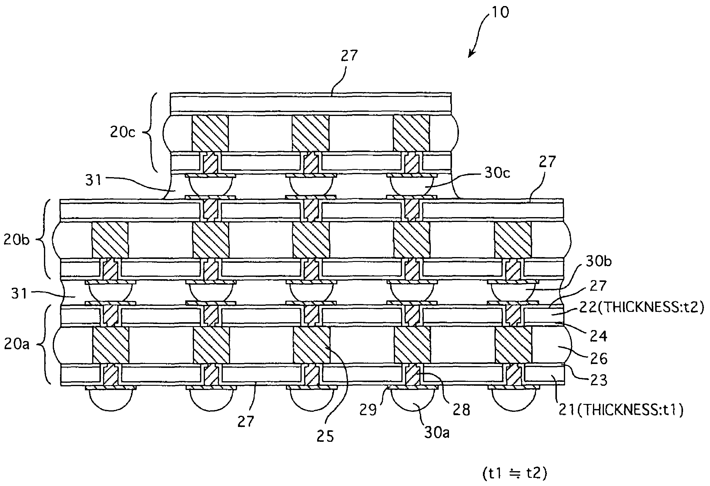
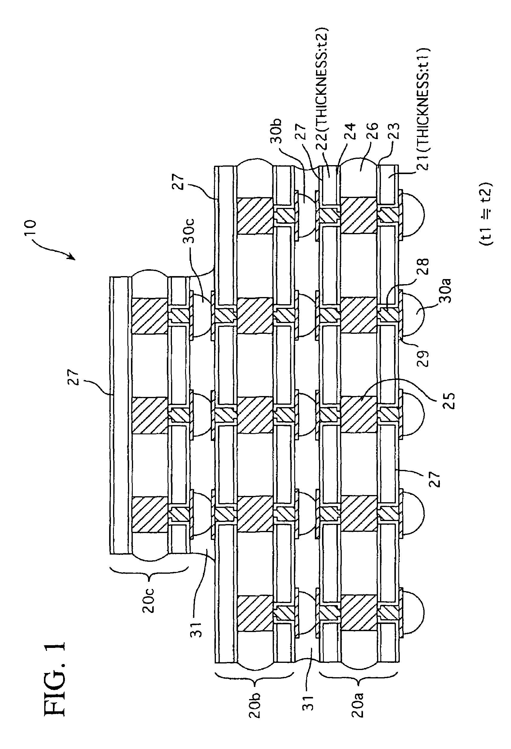
[0026]FIG. 1 schematically shows the sectional structure of a semiconductor device according to an embodiment of the present invention.

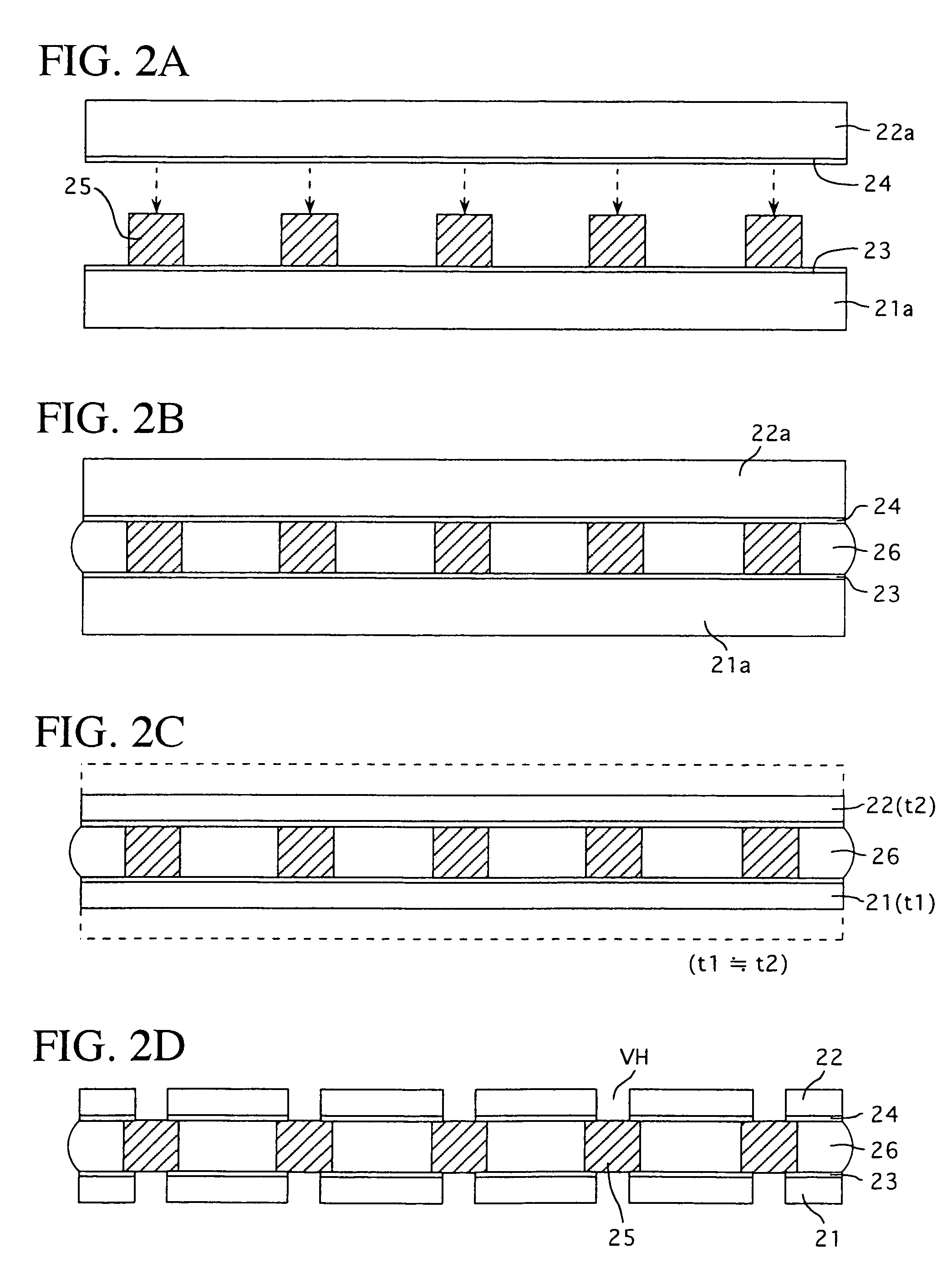
[0027]The semiconductor device 10 according to this embodiment has a three-dimensionally mounted configuration formed by stacking structures 20a, 20b, 20c in three stages, as shown in the figure. In each of the structures 20a, 20b, 20c, numerals 21 and 22 denote a silicon substrate thinned to a prescribed thickness, respectively; numerals 23 and 24 denote a conductor layer which is formed on one surface of the corresponding silicon substrate 21, 22, respectively, and which involves device patterns including required circuit patterns, wiring patterns, or the like; the numeral 25 denotes a metal bump which bonds the two silicon substrates 21, 22 through each of the conductor layers 23, 24 as will be described later; and numeral 26 denotes an insulative resin layer formed by being filled into a gap between the conductor layers 23, 24 bonded together by ...


PUM


Abstract

Two semiconductor substrates are first bonded together by means of a metal bump, while respective one-side surfaces on which device patterns are formed are faced each other, and a resin is then filled into a gap between the respective one-side surfaces and thereafter each of the semiconductor substrates is polished and thinned to a prescribed thickness. Furthermore, a via hole and an insulating film are formed; part of a portion in contact with the metal bump, of the insulating film, is opened; the inside of the via hole is filled with a conductor; and an electrode pad is formed on the conductor, to thereby form structures. Finally, a required number of structures are electrically connected with each other through the electrode pad and stacked to thereby obtain a semiconductor device.

Description

[0001]This application is a divisional application of prior application Ser. No. 10 / 445,821, filed on May 28, 2003 now abandoned.BACKGROUND OF THE INVENTION[0002]1. Field of the Invention[0003]The present invention relates to a semiconductor device and its manufacturing method and, more particularly, to a technique adapted to eliminate drawbacks arising in association with a thinning in performing three-dimensional mounting intended for the high density design and multiple-pin design of semiconductor devices.[0004]2. Description of the Related Art[0005]Conventionally, various methods have been proposed as techniques for accomplishing the high density design and multiple-pin design of semiconductor devices. As one method, for example, there is an available method which involves fabricating a printed wiring board of multilayer structure by means of a build-up method and mounting elements such as semiconductor chips on the multilayer printed wiring board so as to obtain a device.[0006]...

Claims


Application Information

Patent Timeline
Patent Type & Authority Patents(United States)
IPC IPC(8): H01L21/00H01L21/98H01L23/48H01L25/18H01L25/065H01L25/07
CPCH01L23/481H01L25/0657H01L25/50H01L2924/01322H01L2225/06513H01L2225/06541H01L2225/06555H01L2224/16145H01L2224/05573H01L2224/05568H01L21/76898H01L23/12
Inventor MASHINO, NAOHIRO
Owner SHINKO ELECTRIC IND CO LTD
Why Eureka
Try Eureka