

Semiconductor device and method for manufacturing the same
a semiconductor and device technology, applied in the direction of semiconductor devices, basic electric elements, electrical appliances, etc., can solve the problems of increased leakage current from a source electrode or a drain electrode, adverse influence on predetermined operation of semiconductor elements, and difficulty in resisting edge shape, etc., to suppress the variation in properties of elements.
- Summary
- Abstract
- Description
- Claims
- Application Information
AI Technical Summary
Benefits of technology
Problems solved by technology
Method used
Image

Examples
example 1
[0036]Example 1 is an example relating to a method for manufacturing a semiconductor device in which a P-type well region having a predetermined depth from a surface of a semiconductor substrate and an impurity region provided from the bottom portion of the above P-type well region in the depth direction of the semiconductor substrate are formed.
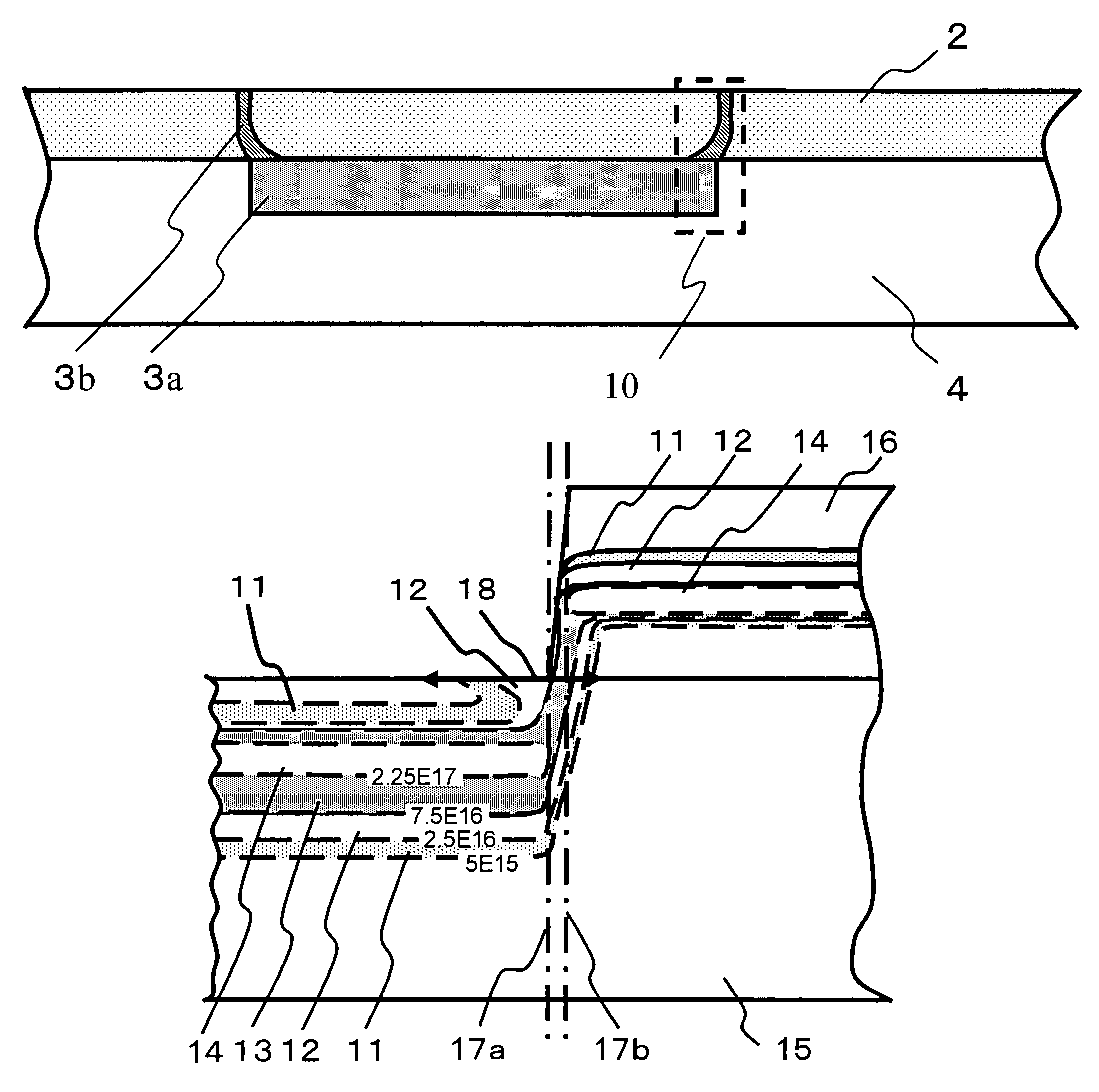
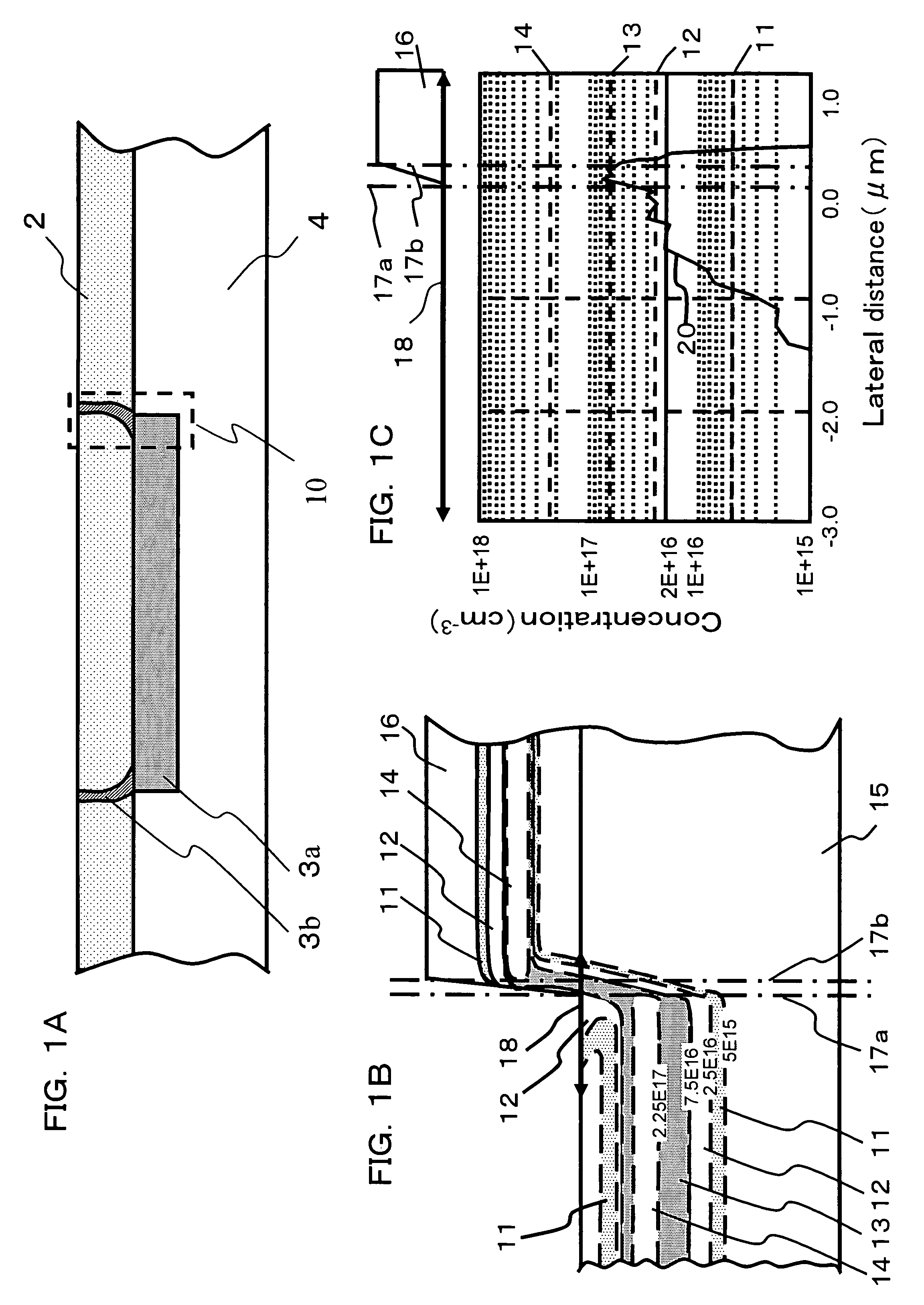
[0037]First, FIGS. 1A, 1B, and 1C are views for illustrating problems in detail of a related method for manufacturing a semiconductor device. In addition, FIG. 1A shows a P-type well region 2, an N-type well region 3a having a large doping depth, a region 3b which is implanted with an impurity passing through a resist, and a P-type semiconductor substrate 4, and a region 10 corresponding to that shown in FIG. 1B.
[0038]In addition, FIG. 1B shows a cross-sectional view of a semiconductor substrate 15 and a resist 16, and in the figure, there are shown isoconcentration lines 11, 12, 13, and 14 indicating concentrations of 5×10¹⁵ / cm3, 2.5×10¹⁶ / c...
example 2
[0069]Example 2 will be described with reference to FIGS. 5A to 5D, 6A to 6D, and 7A to 7D.
[0070]As shown in the above figures, Example 2 is an example relating to a method for manufacturing a semiconductor device in which there are formed a well region having a predetermined depth from a surface of a semiconductor substrate, one impurity region formed in the semiconductor substrate from the bottom portion of the above well region in the depth direction of the substrate, and a semiconductor element formed in the well region and in a boundary area of said one impurity region when viewed in plan.
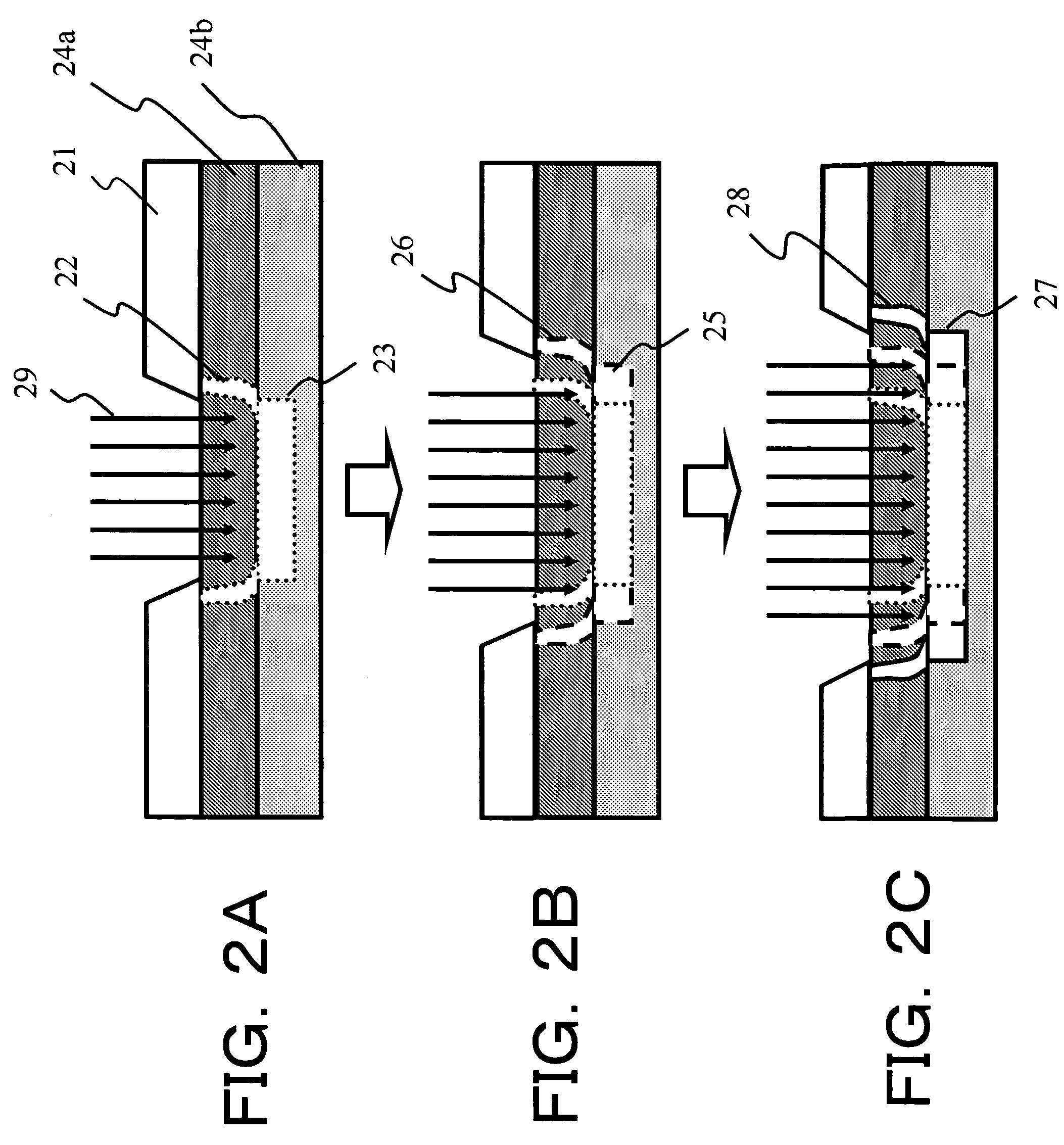
[0071]FIGS. 5A to 5D are views for illustrating a method for manufacturing a semiconductor device, according to Example 2. In the manufacturing method described above, when a P-type well region or an N-type well region formed in the semiconductor substrate from the surface thereof, and an active element formed in the P-type well region or the N-type well region and in the boundary area of one ...
example 3
[0091]With reference to FIGS. 8A to 8C, 9A and 9B, 10A to 10D, 11A to 11D, 12A to 12D, and 13A to 13D, Example 3 will be described. Example 3 is an example relating to a method for manufacturing a semiconductor device in which a triple well structure is formed and CMOS transistors are provided in this triple well, and in this example, one impurity region forming a triple well structure is formed by high-energy ion implantation of an impurity.
[0092]First, with reference to FIGS. 8A, 8B, and 8C, problems of a related method for manufacturing a semiconductor device will be described in detail. FIG. 8A shows an N-type well region 80 having a small doping depth, a P-type well region 81a forming a triple well structure, a P-type well region 81b not forming a triple well structure, an N-type well region 82a having a large doping depth, a region 82b which is implanted with an impurity passing through a resist, a P-type semiconductor substrate 83, a gate electrode and a channel region 84 of ...
PUM
 Abstract
Description
Claims
Application Information