Pixel circuit using direct charging and that performs light-emitting device compensation

a technology of light-emitting device and direct charging, which is applied in the direction of static indicating device, cathode-ray tube indicator, instruments, etc., can solve the problem that the size required by many circuit configurations may not be suitable for high resolution, the brightness of the oled sub-pixel is not wanted, and the drive transistor properties are not applicable to performan

Active Publication Date: 2020-09-01
SHARP KK
View PDF10 Cites 0 Cited by
  • Summary
  • Abstract
  • Description
  • Claims
  • Application Information

AI Technical Summary

Benefits of technology

[0007]The present invention relates to pixel circuits that employ charge-based programming configurations that eliminate the need for a drive transistor, and also are capable of compensating for variations in the properties of the OLED, including the OLED threshold voltage for light emission. The described circuit configurations employ an external compensation system and methods to compensate for the OLED device variations.
[0010]Circuit configurations in accordance with the present disclosure have advantages over conventional configurations. The charge-based programming configurations and methods enable programming data and light emission without requiring a drive TFT, i.e. there is no drive TFT operating in an analogue mode to control the current delivered to the OLED. This removes the deleterious effects of variations in drive TFT characteristics. In addition, unlike conventional charge-based programming configurations, the configurations and methods of the present disclosure compensate for variations in OLED characteristics, including OLED threshold voltage.

Problems solved by technology

Accordingly, even if the gate voltage is the same between two different drive TFTs, the amount of current delivered by the drive TFT to the OLED may vary by a large amount, causing an unwanted variation in the brightness of the OLED sub-pixel.
The size required by many of these circuit configurations may not be suitable for high resolution (e.g. high pixels per inch or ppi) display applications, in which each subpixel must occupy only a small area.
Such a configuration that operates by charge-based programming lacks the analogue drive transistor of other conventional configurations, and thus variations of drive transistor properties will not be applicable to performance.
Conventional charge-based programming configurations such as described above, however, do not compensate the OLED variations.
This type of current source may be difficult to realize in practice when the current source must supply the current to a large number of sub-pixels in a column, such as in a display device.
In particular for low current circumstances or applications, the drive speed could be detrimentally slow.

Method used


Image

  • Pixel circuit using direct charging and that performs light-emitting device compensation
  • Pixel circuit using direct charging and that performs light-emitting device compensation
  • Pixel circuit using direct charging and that performs light-emitting device compensation

Examples


Embodiment Construction

[0029]Embodiments of the present invention will now be described with reference to the drawings, wherein like reference numerals are used to refer to like elements throughout. It will be understood that the figures are not necessarily to scale.

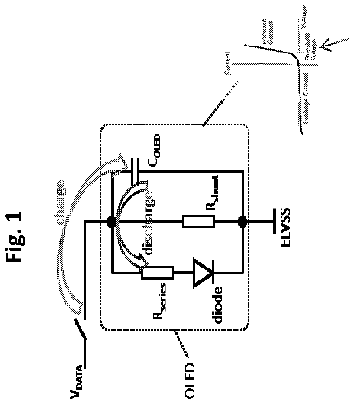
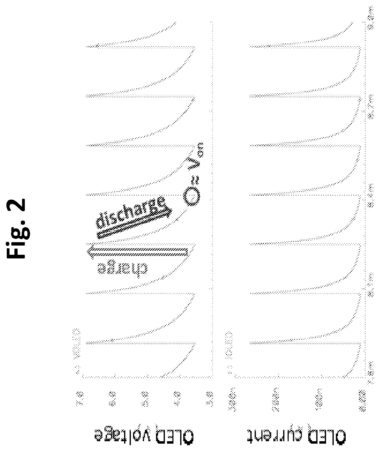
[0030]The present invention employs pixel circuits that use charge-based programming configurations that eliminate the need for a drive transistor (TFT), and also are capable of compensating for variations in the properties of the OLED, including the OLED threshold voltage for light emission. The OLED threshold voltage generally is the minimum voltage across the OLED for which the current passed by the OLED is above a particular value for light emission. In a charge programming configuration, the total light energy output (L) is proportional to the total charge (Q) delivered to the OLED, which is equal to the current through the OLED (I) multiplied by the emission time (t):

L=k·(I·t)=kQ

where k is a constant of proportionality.

[0031]In conventi...


PUM


Abstract

A display system includes a display panel comprising a plurality of pixel circuits, and a measurement and data processing unit that is external to the display panel. Each pixel circuit includes a light-emitting device having a first terminal connected to a first voltage supply and a second terminal opposite from the first terminal; a first transistor connected between a data voltage supply line from the measurement and data processing unit and the second terminal of the light emitting device; and a second transistor connected between the second terminal of the light-emitting device and a sample line to the measurement and data processing unit. The measurement and data processing unit samples a measured voltage at the second terminal of the light-emitting device through the sample line and outputs a data voltage to the light-emitting device based on the measured voltage to compensate variations in properties of the light-emitting device.

Description

TECHNICAL FIELD[0001]The present invention relates to design and operation of electronic circuits for delivering electrical current to an element in a display device, such as for example to an organic light-emitting diode (OLED) in the pixel of an active matrix OLED (AMOLED) display device.BACKGROUND ART[0002]Organic light-emitting diodes (OLED) generate light by re-combination of electrons and holes, and emit light when a bias is applied between the anode and cathode such that an electrical current passes between them. The brightness of the light is related to the amount of the current. If there is no current, there will be no light emission, so OLED technology is a type of technology capable of absolute blacks and achieving almost “infinite” contrast ratio between pixels when used in display applications.[0003]In many conventional configurations, the OLED in the sub-pixel of a display is driven by an analogue drive transistor (drive TFT), which is in series with the OLED. The amou...

Claims


Application Information

Patent Timeline
Patent Type & Authority Patents(United States)
IPC IPC(8): G09G5/10G09G3/3258
CPCG09G3/3258G09G2300/0819G09G2300/0828G09G2300/0852G09G2320/029G09G2320/0233G09G3/32G09G3/006
Inventor LU, TONGBROWNLOW, MICHAEL JAMESSMEETON, TIM MICHAEL
Owner SHARP KK
Why Eureka
Try Eureka