
Method for carbon nanotube emitter surface treatment

Inactive Publication Date: 2010-02-16
IND TECH RES INST
View PDF7 Cites 0 Cited by
  • Summary
  • Abstract
  • Description
  • Claims
  • Application Information

AI Technical Summary

Benefits of technology

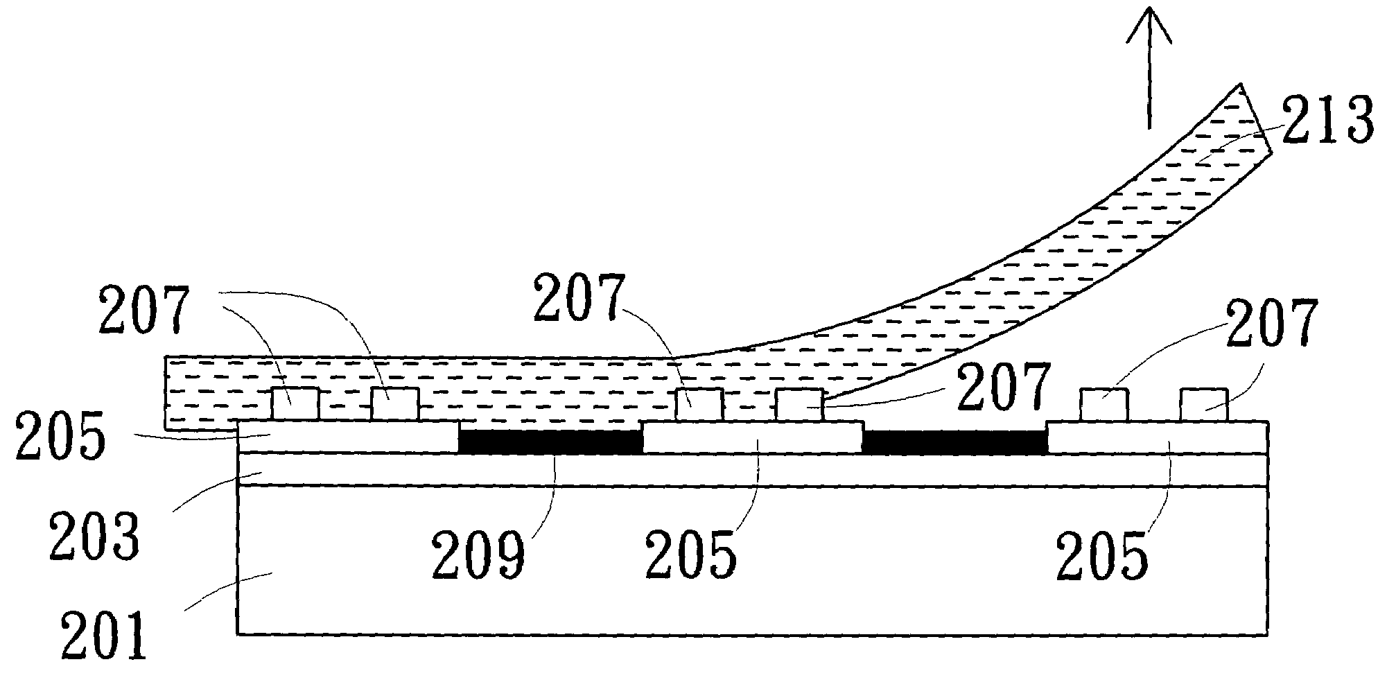
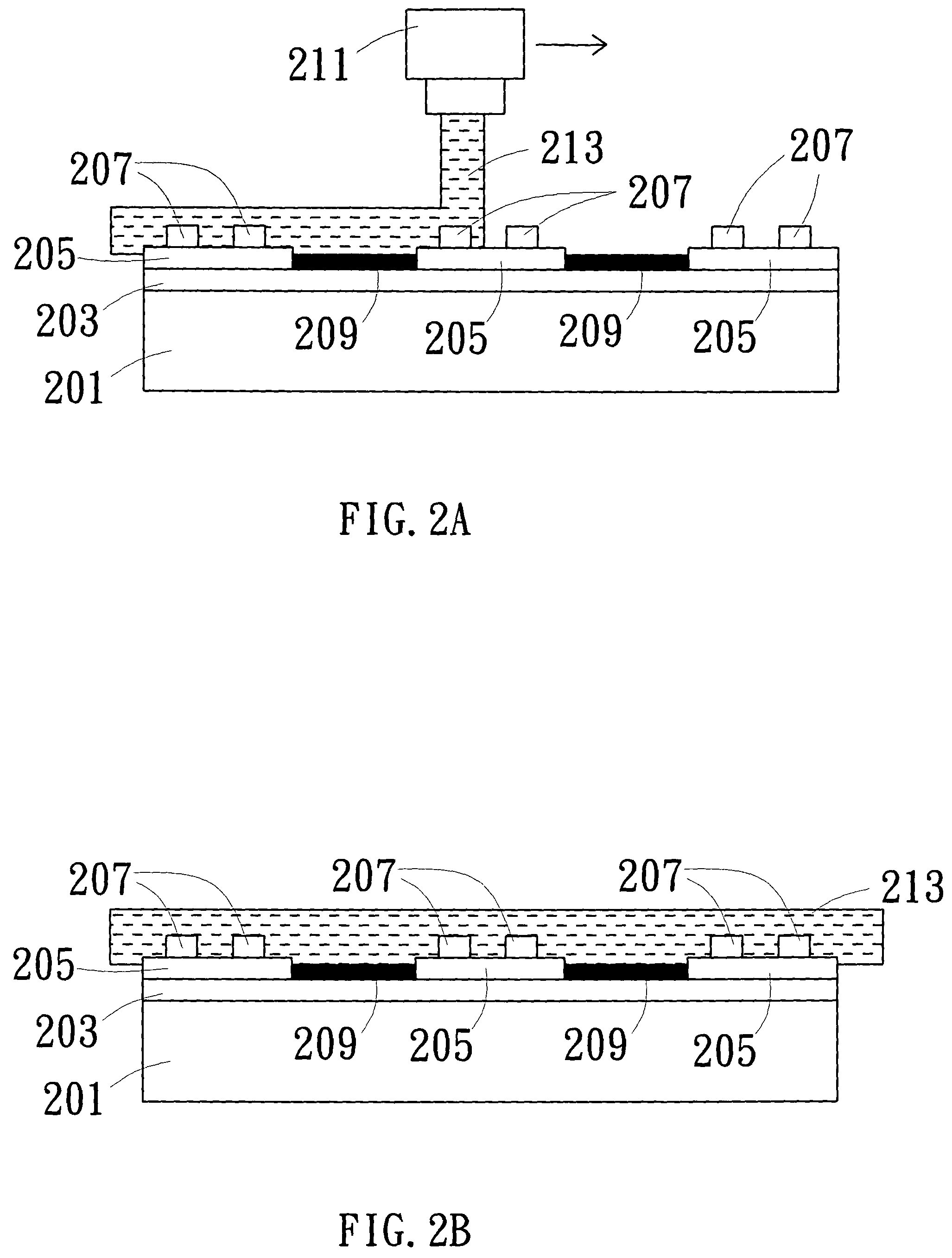
[0008]It is a primary object of the present invention to provide a method for carbon nanotube emitter surface treatment, which is used to increase the number of carbon nanotubes exposed on the triode structure device. For advancing the current density and intensity of CNT emitters, the invention uses a method of casting surface treatment on the CNT emitters including the steps of coating an adhesive material on the surface of device; heating the adhesive material for adhibitting the surface; and lifting the adhesive material off.
[0009]The casting surface treatment of the present invention can process the CNT electronic source in the triode or any structure to improve the uniformity of the surface of the CNTs on the carbon nanotube field emitter display in any kind of structure, and then increase the number of the CNTs exposed on the device.

Problems solved by technology

However, the drawback of the prior art is in the problem associated with the uniformity of the field emission electronic source.

Method used


Image

  • Method for carbon nanotube emitter surface treatment
  • Method for carbon nanotube emitter surface treatment
  • Method for carbon nanotube emitter surface treatment

Examples


Embodiment Construction

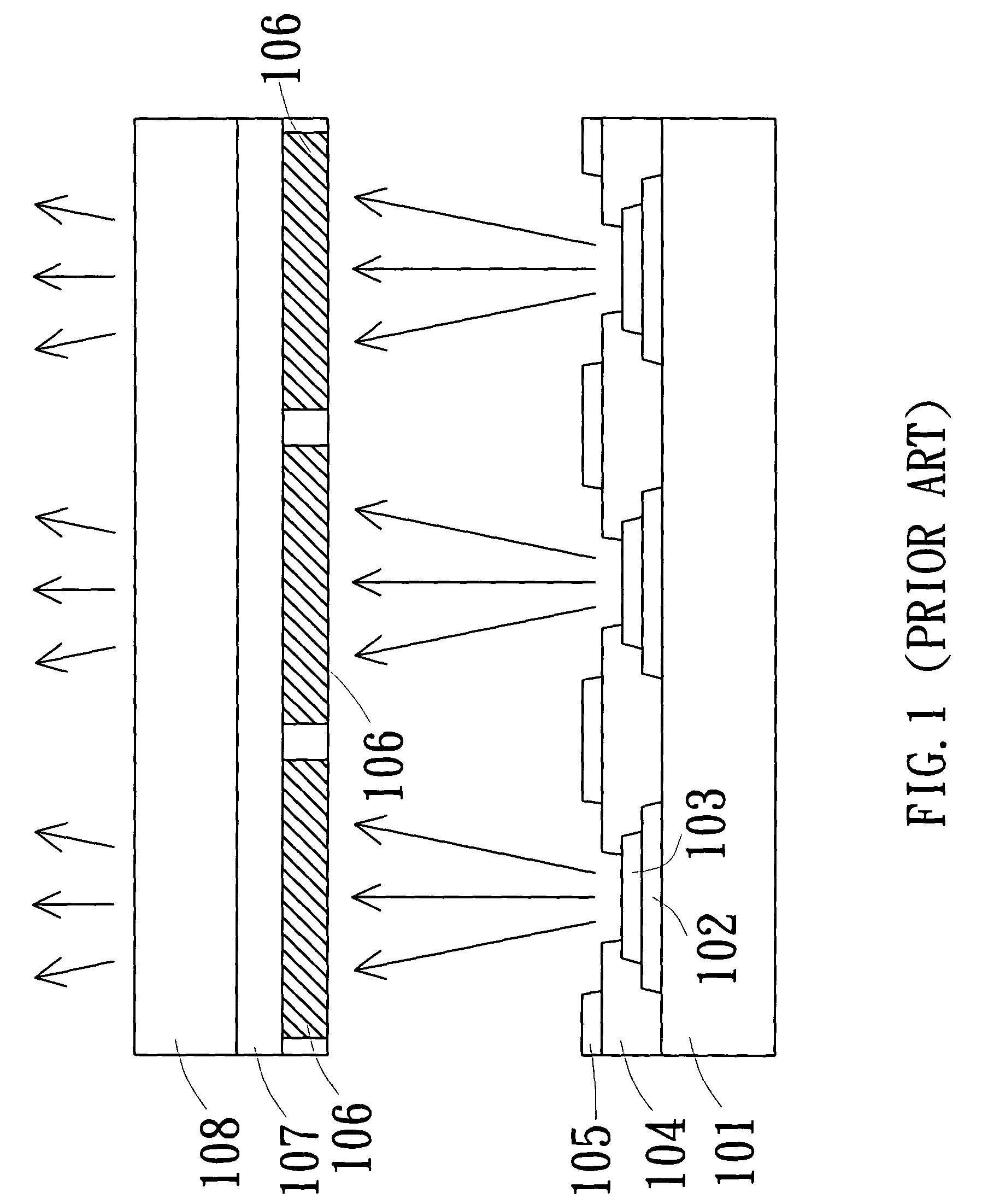
[0019]In the triode structure of carbon nanotube field emission display (CNT-FED), the invention adopts a method for casting surface treatment to increase the number of carbon nanotubes exposed on the surface of the device. And the invention also can advance the current density and intensity of the CNT emitters in the gate hole formed around the CNT electronic source in the triode or any structure of CNT-FED so that the CNT emitters can emit the electronics in high-density and great-intensity uniformly.

[0020]The method of surface treatment comprises the steps below:

[0021]Please refer to FIG. 2A to FIG. 2C, which are schematic diagrams showing the method for carbon nanotube emitter surface treatment in accordance with the first preferred embodiment of the present invention. The figures show a triode structure of CNT-FED using the manufacturing process of semi-conductor thin film. First, with reference to the FIG. 2A, there is a two-dimension distribution cathode plate 203 fabricated ...


PUM


Abstract

A method for increasing the number of carbon nanotubes exposed on the triode structure device of a field emission display uses the technology of casting surface treatment. For advancing the current density and magnitude of CNT emitters, the method of casting surface treatment on the CNT emitters includes the steps of coating an adhesive material on the surface of the device; heating the adhesive material for adhibitting the surface; and lifting the adhesive material off the surface.

Description

BACKGROUND OF THE INVENTION[0001]1. Field of the Invention[0002]The invention relates to a method for carbon nanotube emitter surface treatment, which is used to increase the number of CNTs (carbon nanotubes) exposed on a field emission display (FED) device for advancing the current density and magnitude of CNT emitters.[0003]2. Description of the Prior Art[0004]To implement a flat panel display, the CNT-FED (carbon nanotube field emission display) adopts the technology of screen-printing process and FED display in the prior art. It not only keeps the image quality of a CRT display, but also the advantage of power-saving and slim-volume, and with the characters of CNTs including low-conducting electronic field required, high density of emission current, and high stability. As a result, it may offer a flat panel display with good luminous efficiency, and large-size screen as well as power-saving and low-cost.[0005]FIG. 1 shows the luminous theory of the triode structure of a carbon n...

Claims


Application Information

Patent Timeline
IPC IPC(8): B05D5/12H01J9/02B05D3/12H01J1/304H01J21/06H01J31/12
CPCB82Y10/00B82Y30/00H01J9/025H01J1/304H01J2201/30469
Inventor SHEU, JYH-RONGLEE, CHUN-TAOLEE, CHENG-CHUNGHO, JIA-CHONGCHANG, YU-YANG
Owner IND TECH RES INST
Learn More