Leadframe-based semiconductor package

a semiconductor and leadframe technology, applied in semiconductor devices, semiconductor/solid-state device details, electrical apparatus, etc., can solve the problems of difficult repositioning of internal leads, delamination, etc., and achieve the effect of enhancing the adhesion of leads

Inactive Publication Date: 2010-02-23
POWERTECH TECHNOLOGY
View PDF5 Cites 11 Cited by
  • Summary
  • Abstract
  • Description
  • Claims
  • Application Information

AI Technical Summary

Benefits of technology

[0006]The main purpose of the present invention is to provide a leadframe-based semiconductor package by partially embedding the internal leads into the second adhesive layer of the multi

Problems solved by technology

Therefore, the internal leads will not easily be shifted nor delaminated due to the impact of the mold flows during molding processes, mo

Method used


Image

  • Leadframe-based semiconductor package
  • Leadframe-based semiconductor package
  • Leadframe-based semiconductor package

Examples


Embodiment Construction

[0024]Please refer to the attached drawings, the present invention is described by means of embodiments below.

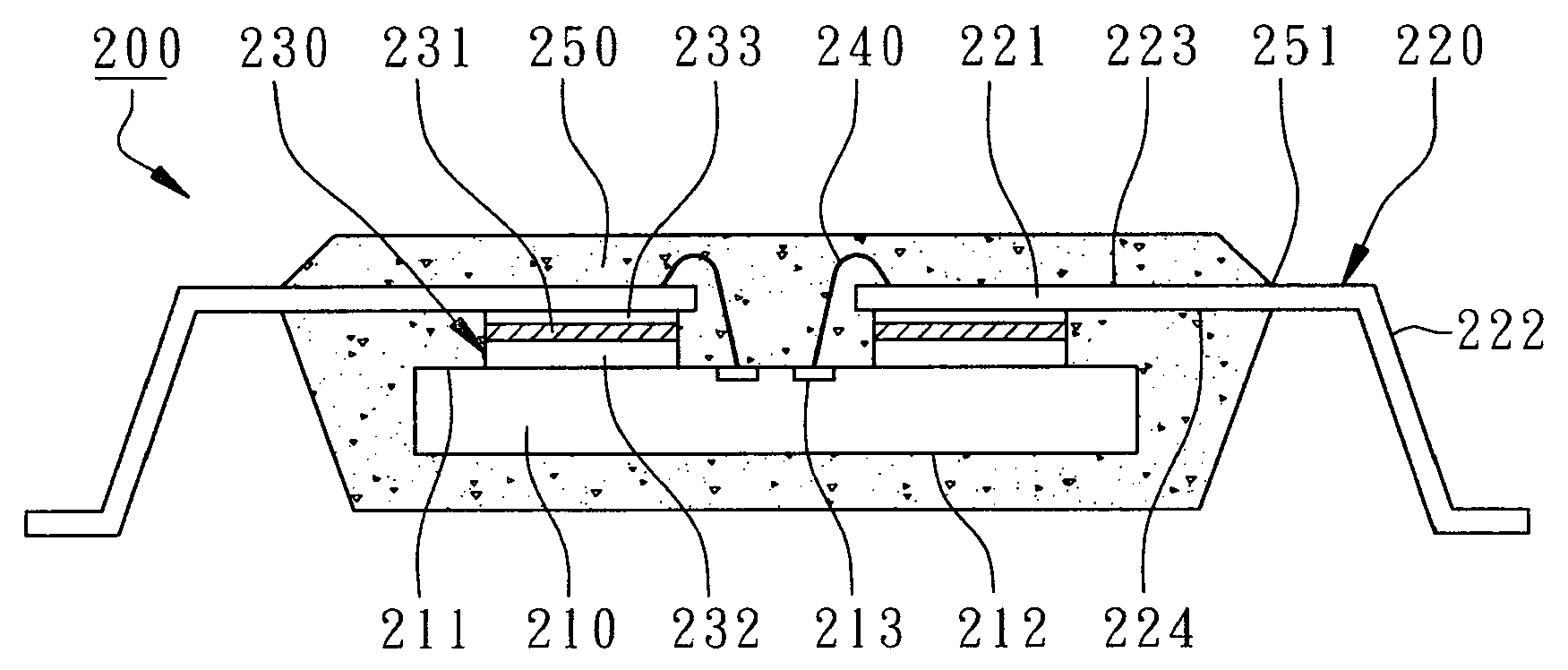
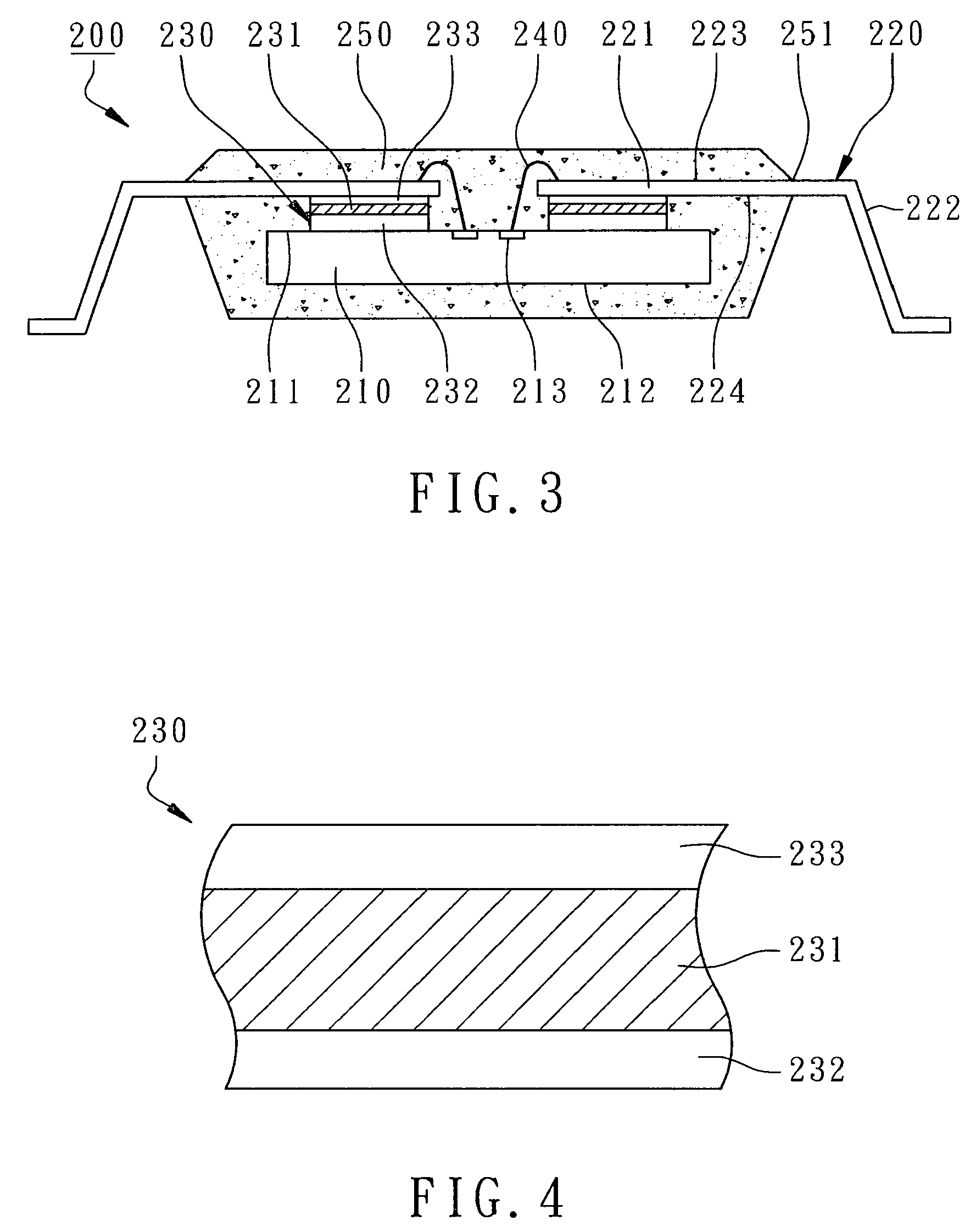
[0025]According to the first embodiment of the present invention, a leadframe-based semiconductor package is illustrated in FIG. 3 for a cross-sectional view. The leadframe-based semiconductor package 200 primarily comprises a chip 210, a plurality of leads 220 of a leadframe, a multi-layer tape 230, a plurality of bonding wires 240, and an encapsulant 250.

[0026]The chip 210 is made of a semiconductor material and includes various micro active components such as IC, MEMS components, optoelectronic components, etc. The chip 210 has an active surface 211 and a corresponding back surface 212 where a plurality of bonding pads 213 are disposed in a single row or multiple rows on the active surface 211 of the chip 210. In this embodiment, the bonding pads 213 are central pads.

[0027]The leads 220 are parts of a leadframe and made of metal having high electrical and thermal conducti...


PUM


Abstract

A leadframe-based semiconductor package is revealed, primarily comprising a chip, a plurality of leads of a leadframe, a multi-layer tape, and an encapsulant. The multi-layer tape is attached to the chip and includes an adhesive layer disposed on a dielectric core layer. The internal leads of the leads are partially embedded in the adhesive layer in a manner not to directly contact the dielectric core layer. A bonding interface with a U-shaped profile is formed between the adhesive layer and each internal lead to increase the adhesions of the leads so that the internal leads will not be shifted nor delaminated during molding processes. The concentrated stresses exerted on the internal leads disposed at the corners of the packages will be released and reduced.

Description

FIELD OF THE INVENTION[0001]The present invention relates to a semiconductor device, especially to a leadframe-based semiconductor package.BACKGROUND OF THE INVENTION[0002]Among well-known semiconductor packages, leadframe-based semiconductor packages have been widely implemented by using leadframes as chip carriers. Advanced leadframes have a plurality of metal leads not only for electrical connections but also for carrying chips by extending metal leads onto chip surfaces to eliminate or shrink the dimension of the die pad of a conventional leadframe. The leadframes with shrunk die pads or without die pads for leadframe-based semiconductor packages can be classified into two different package types, Lead-On-Chip (LOC) and Chip-On-Lead (COL), where “Lead-On-Chip” means to attach the leads to the active surface of a chip and “Chip-On-Lead” means to attach the back surface of a chip to the middle sections of the leads. However, no matter it is an LOC package or a COL package, it is v...

Claims


Application Information

Patent Timeline
IPC IPC(8): H01L23/495
CPCH01L23/4951H01L23/49551H01L24/29H01L24/32H01L24/83H01L23/49513H01L2924/1461H01L23/49555H01L24/45H01L24/48H01L2224/29007H01L2224/2919H01L2224/32014H01L2224/32245H01L2224/45124H01L2224/45144H01L2224/45147H01L2224/48091H01L2224/48247H01L2224/4826H01L2224/73215H01L2224/73265H01L2224/83101H01L2224/83194H01L2224/83855H01L2224/83856H01L2224/8388H01L2924/01005H01L2924/01013H01L2924/01029H01L2924/01075H01L2924/01079H01L2924/01082H01L2924/07802H01L2924/00013H01L2224/29H01L2224/29298H01L2924/01006H01L2924/01033H01L2924/0665H01L2924/00014H01L2924/00H01L2224/29099H01L2224/29199H01L2224/29299H01L2224/2929H01L2924/351H01L2924/181H01L2224/2612H01L2924/00012
Inventor FAN, WEN-JENG
Owner POWERTECH TECHNOLOGY
Why Eureka
Try Eureka