

Coupling antenna
a coupling antenna and antenna technology, applied in the direction of elongated active element feed, resonant antenna, radiating element structure, etc., can solve the problems of limited practical application of the antenna, small area of the antenna generating capacitive coupling effect, etc., and achieve wide bandwidth and small size
- Summary
- Abstract
- Description
- Claims
- Application Information
AI Technical Summary
Benefits of technology
Problems solved by technology
Method used
Image

Examples
Embodiment Construction
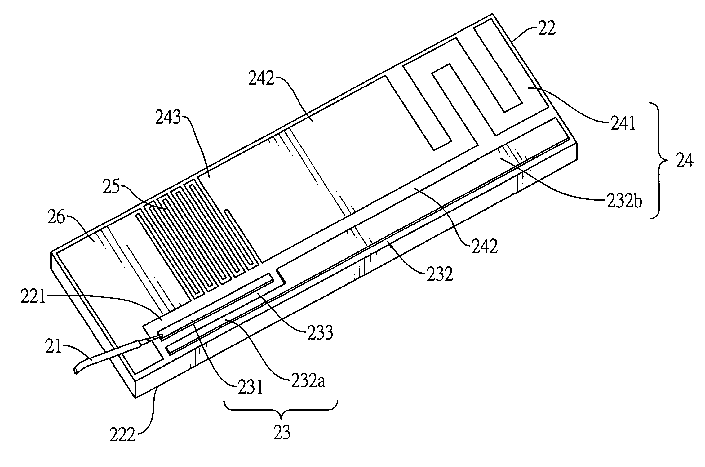
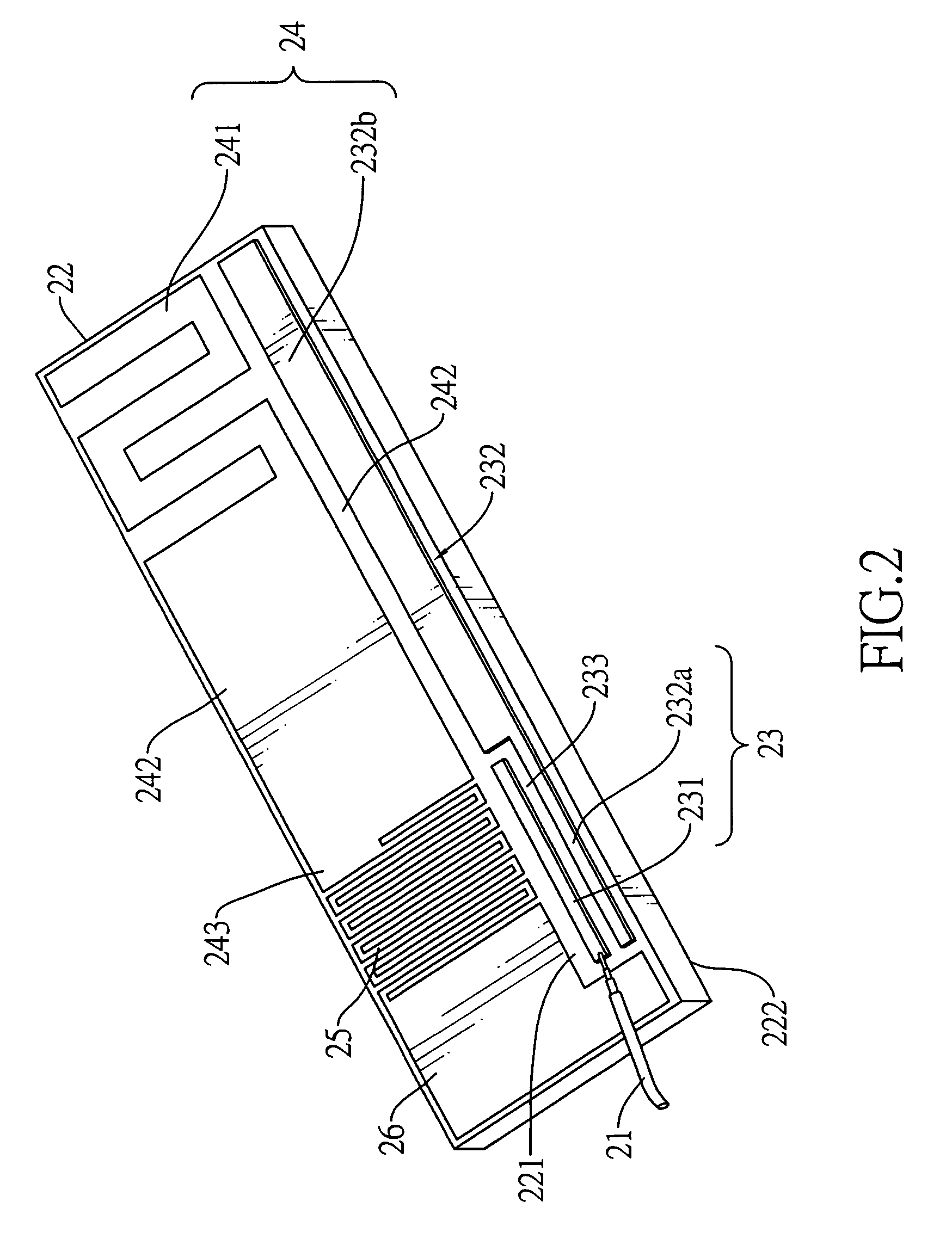
[0016]With reference to FIGS. 2 and 3, a first embodiment of a coupling antenna in accordance with the present invention is connected to a feeding cable (21) and comprises a substrate (22), a feeding conductor (231), a coupling conductor (232), a mating conductor (241), an extension conductor (242), an inducting conductor (25), a ground plane (26), a first coupling member (23) and a second coupling member (24).
[0017]The substrate (22) is made of dielectric material and has a top surface (221) and a bottom surface (222). The dimension of the substrate (22) has the length of about 76 mm, the width of about 9 mm and the thickness of about 0.2 mm.
[0018]The feeding conductor (231) is made of metal, is mounted on the top surface of the substrate (22) and is connected to the feeding cable (21) to receive signals from the feeding cable (21). The dimension of the feeding conductor (231) has the length of about 15 mm and the width of about 1 mm.
[0019]The coupling conductor (232) is made of me...
PUM
 Abstract
Description
Claims
Application Information