Scalable wideband probes, fixtures, and sockets for high speed IC testing and interconnects

a wideband, probe technology, applied in the direction of instruments, semiconductor devices, measurement devices, etc., can solve the problems of fewer and more costly remedies, if any, and the failure of semiconductor chips in any of these stages, so as to reduce cross talk and prasitics, wide bandwidth, and high speed

Active Publication Date: 2008-10-30
WAYMO LLC
View PDF4 Cites 94 Cited by
  • Summary
  • Abstract
  • Description
  • Claims
  • Application Information

AI Technical Summary

Benefits of technology

[0006]These and other problems are solved by a Periodic Micro Coaxial Transmission Line (PMTL) described herein provides Confined Field Interconnection (CFI) between devices in wafer and on a high speed board, thus, substantially reducing cross talk and prasitics and allowing relatively higher speeds and wider bandwidth. In one embodiment, the PMTL is used in connection with semiconductor test and evaluation of wafers and single chips resulting from wafer cutting in various stages of development including packaging, wire bounding, socket and the like.

Problems solved by technology

A failure of semiconductor chip in any of these stages can be rather damaging.
If they fail, the whole system will fail, and the remedies, if any, are fewer and more costly.
The failure is often more catastrophic and costly as the level of integration increases.
As the designers build more complexities into these chips, the need for improved test equipment becomes even more critical.

Method used


Image

  • Scalable wideband probes, fixtures, and sockets for high speed IC testing and interconnects
  • Scalable wideband probes, fixtures, and sockets for high speed IC testing and interconnects
  • Scalable wideband probes, fixtures, and sockets for high speed IC testing and interconnects

Examples


Embodiment Construction

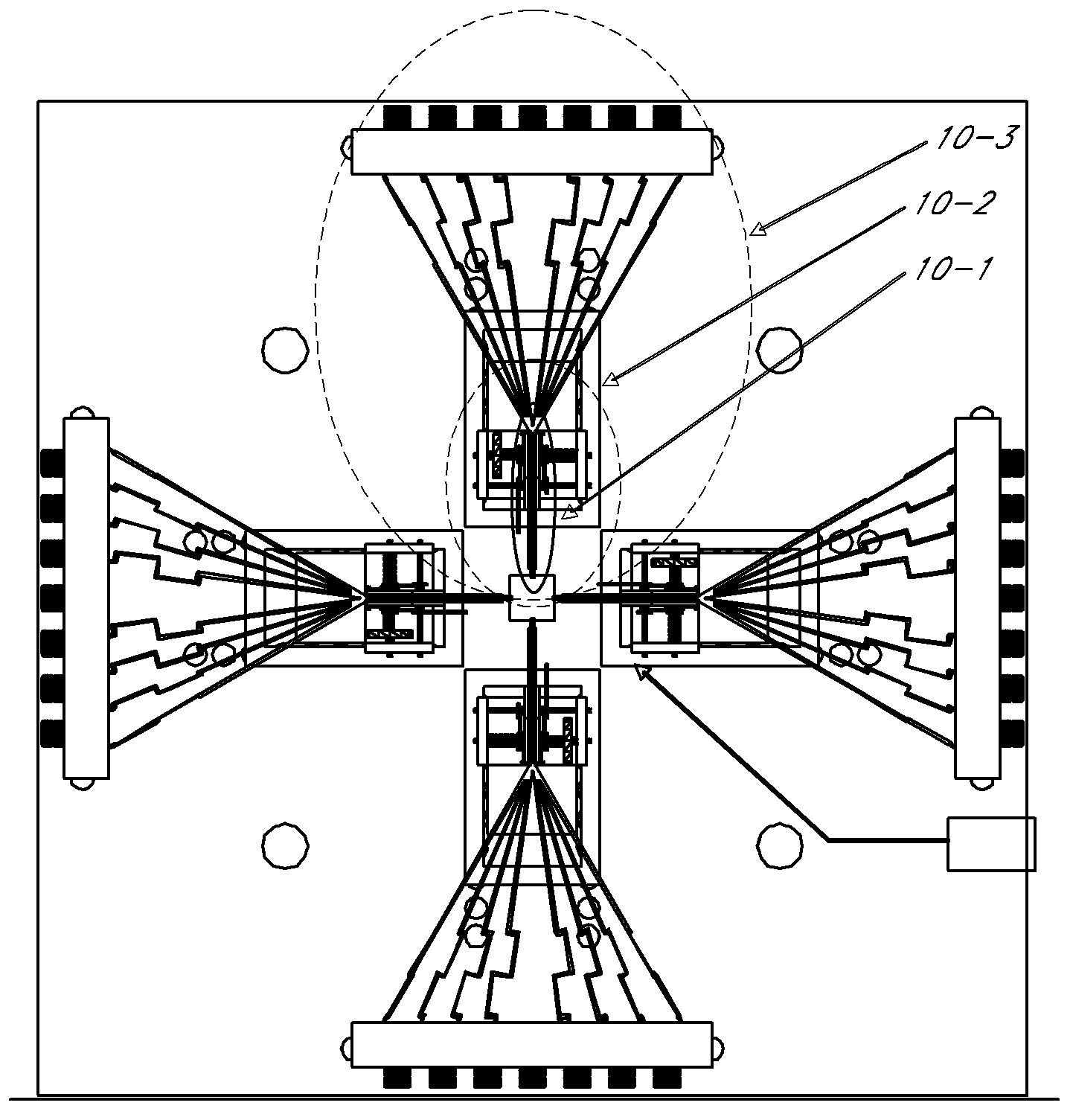
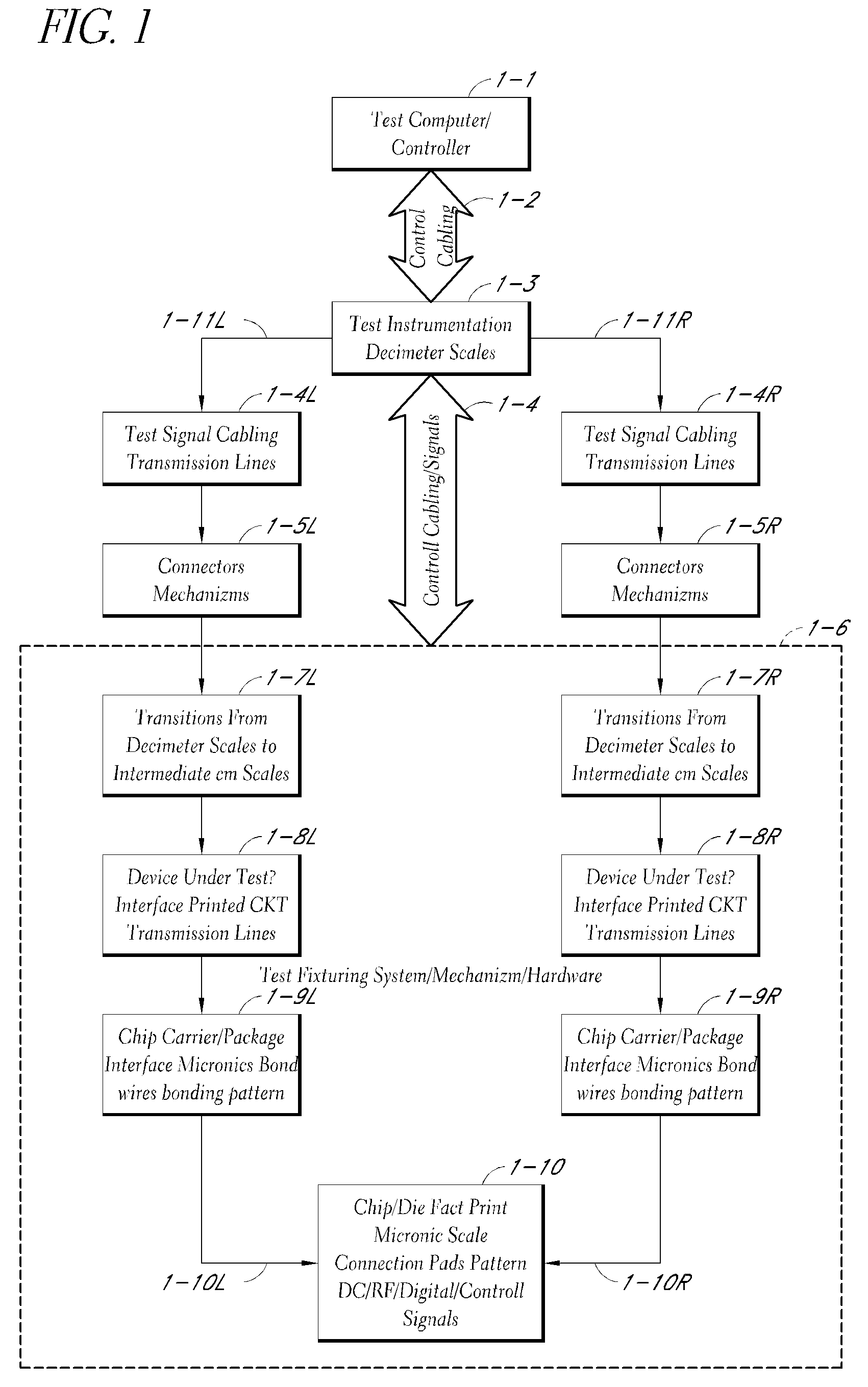
[0138]The block diagram of FIG. 1 summarizes the process of semiconductor chip testing and evaluation. On the top level, the test system includes test instrumentation that generates the signal stimulus, typically an HP8510 vector network analyzer or other similar equipment. This instrumentation usually has high-precision input and output ports that are of coaxial nature. This is represented by block 1-3 in FIG. 1. This instrumentation can be controlled by a test computer 1-1 for automation purposes connected to the test instrumentation 1-3 through control bus 1-2. The test signals are provided by the test instrument 1-3 through cable 1-11L to the test signal cabling 1-4L, which is then supplied to a connector mechanism 1-5L. The functional test fixture System Mechanism and Hardware is lumped into a block 1-6 to indicate a boundary beyond which the test instrument signal will interconnect. The connections on the left represent the flow path of the input of the stimulus from the test ...


PUM


Abstract

We introduce a new Periodic micro coaxial transmission line (PMTL) that is capable of sustaining a TEM propagation mode up to THz band. The PMTL can be manufactured using the current photolithographic processes. This transmission line can be embedded in microscopic layers that allow many new applications. We use the PMTL to develop a wideband highly scalable connector that is then used in a Probe that can be used for connecting to microscopic scale Integrated Circuits with picoseconds High Speed Digital and near THz Analogue performance in various stages of development from R&D to production testing. These probes, in one embodiment, provide a thin pen-like vertical probe tip that matches the die pad pattern precisely that can be as agile as a high speed plotter pen, connecting on the fly to any die pattern on a wafer. This approach allows the most valuable part of the test, namely the wafer to remain stationary and safe, and the least costly part of the test, namely the probe to take most of the wear and tear. We further use the embedded PMTL to develop a modular, scaleable and fully automated Universal Test Fixture for testing chips in various stages of development mainly for digital IC chips that can be utilized in production lines with pick and place of chips on tape to test every chip before insertion into circuits. One embodiment includes a low profile wideband Signal Launcher and an alligator type RF Clip that can be used at the edge of PCB's directly for validation broads. The Signal Launcher is used to develop a new versatile Flush Top Test Fixtures for individual device testing in various stages of development from die, to packaged, to Module, to Circuit Boards. The PMTL can also provide Confined Field Interconnects (CFI) between various elements on semiconductor wafers to reduce parasitic and radiation losses and practically eliminating cross talk, thus, increasing the speed of digital IC's. The PMTL is also used to develop a Universal Test Socket, and a Hand Probe with performance up to 220 GHz.

Description

REFERENCE TO RELATED APPLICATIONS[0001]The present application claims priority to U.S. Provisional Application No. 60 / 909,685, filed Apr. 2, 2007, titled “SCALABLE WIDEBAND PROBES, FIXTURES, AND SOCKETS FOR HIGH SPEED IC TESTING AND INTERCONNECTS,” the entire contents of which is hereby incorporated by reference.BACKGROUND OF THE INVENTION[0002]1. Field of the Invention[0003]The invention relates to probes and / or fixtures for testing and using integrated circuits.[0004]2. Description of the Related Art[0005]The cycle of the semiconductor product development includes: wafer processing, wafer testing, probing, cutting into single devices / chips, packaging devices, circuit insertion, module insertion, subsystem insertion, and system integration. A failure of semiconductor chip in any of these stages can be rather damaging. But the earlier the problem is identified, the sooner and less disastrous the consequence will be. In the product cycle, the chips are bare and easy to get to, even i...

Claims


Application Information

Patent Timeline
Patent Type & Authority Applications(United States)
IPC IPC(8): G01R31/02
CPCG01R1/045G01R1/06744G01R1/06772G01R1/06727H01L2224/05553H01L2224/48091H01L2224/48247H01L2224/49171H01L2924/00014
Inventor IZADIAN, JAMAL S.
Owner WAYMO LLC
Why Eureka
Try Eureka