Method of manufacturing film bulk acoustic resonator using internal stress of metallic film and resonator manufactured thereby

a technology of acoustic resonators and metallic films, which is applied in the direction of bulk negative resistance effect devices, electrical equipment, semiconductor devices, etc., can solve the problems of fundamentally impossible to construct saw filter with an mmic structure, deterioration of yield rate, and limitations of dielectric filters in minimizing siz

Active Publication Date: 2010-03-02
SAMSUNG ELECTRONICS CO LTD
View PDF14 Cites 18 Cited by
  • Summary
  • Abstract
  • Description
  • Claims
  • Application Information

AI Technical Summary

Benefits of technology

[0018]Therefore, it is an aspect of the present invention to provide a method of manufacturing a film bulk acoustic resonator and the resonator manufactured thereby through applying external forces when depositing upper / lower electrode layers and generating a stress upward so that the upper / lower electrode layers and piezoelectric layers can be spaced from a semiconductor substrate without requiring a separate supporter or a holder.
[0019]It is another aspect of the present invention to provide a method of manufacturing a film bulk acoustic resonator and the resonator manufactured thereby through forming wrinkles in a predetermined area of a lower electrode layer so that a piezoelectric structure can be spaced from a semiconductor substrate to be higher than a predetermined height even by a slight upward stress generated by a small amount of external force.

Problems solved by technology

However, the dielectric filter has limitations in minimizing its size and realizing monolithic microwave ICs (MMIC) that are recent trends in technical development.
Moreover, it is fundamentally impossible to construct the SAW filter with an MMIC structure, which is adopted for a semiconductor substrate, and with a single chip.
However, the FBAR of the bulk micro machining type also has drawbacks in that an element occupies a large area due to the orientation of the semiconductor substrate and a yield rate is deteriorated due to breaking caused by low structural stability in the post packaging process.
However, it also poses problems in that it is difficult to control the thickness between the layers to realize total reflection and manufacturing cost increases to form a reflection layer for the acoustic reflection 28.
However, it has drawbacks of a deteriorating low yield rate and easy breakability in the post process because of long exposure of the structure when etching the sacrificial layer as well as being a complicated manufacturing process.

Method used


Image

  • Method of manufacturing film bulk acoustic resonator using internal stress of metallic film and resonator manufactured thereby
  • Method of manufacturing film bulk acoustic resonator using internal stress of metallic film and resonator manufactured thereby
  • Method of manufacturing film bulk acoustic resonator using internal stress of metallic film and resonator manufactured thereby

Examples


Embodiment Construction

[0034]Exemplary embodiments of the present invention will be described below with reference to the accompanying drawings. In the following description, well-known functions or constructions are not described.

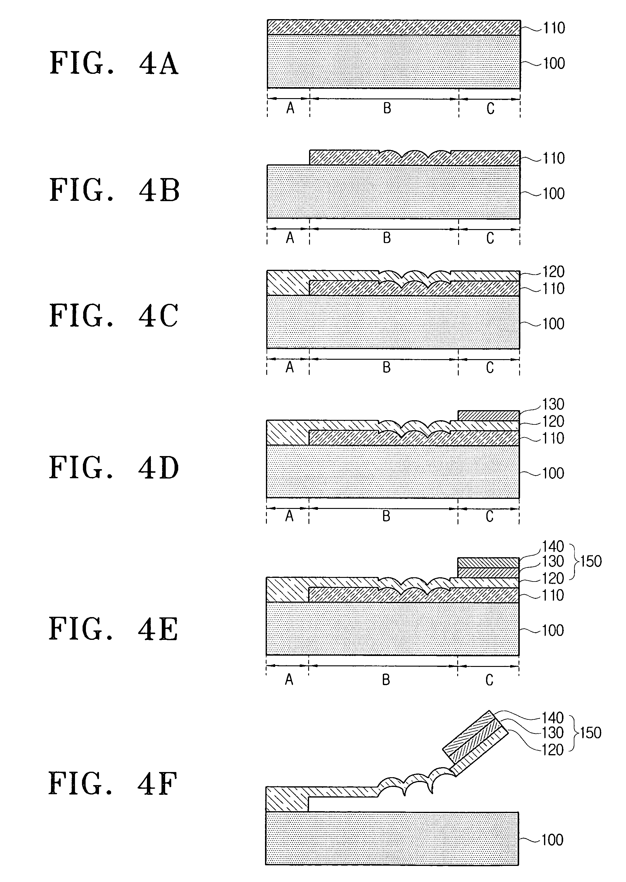
[0035]FIGS. 4A to 4F are diagrams illustrating a series of a manufacturing process according to an exemplary example of the present invention.

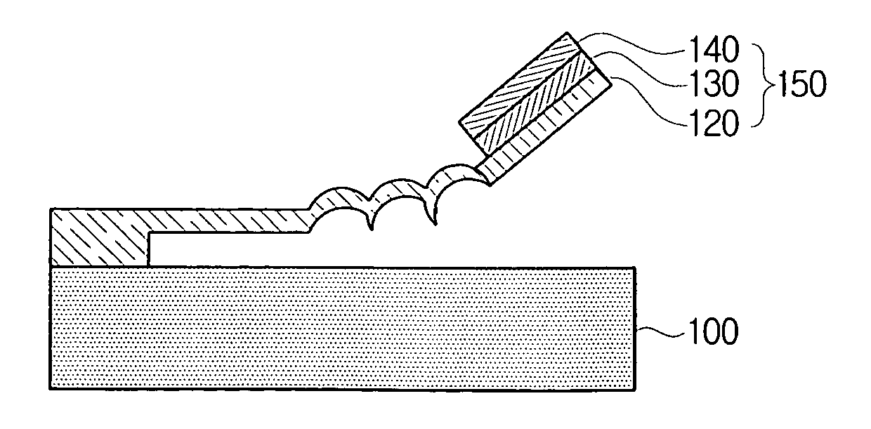
[0036]For descriptive convenience, the structure comprising upper / lower electrode layers 120, 140 and a piezoelectric layer 130 formed in the process below will be referred to a piezo-resonance structure 150. Based on that definition, description will now be made by dividing the piezo-resonance structure 150 into three areas, i.e., a conductive area A, a resonance area C, and a supporting area B.

[0037]The conductive area A is an area, in which the piezo-resonance structure 150 is electrically in contact with a signal line (not shown) of the semiconductor substrate 100. The upper / lower electrode layers 120, 140 and the piezoelectric layer 1...


PUM

PropertyMeasurementUnit
widthaaaaaaaaaa
radio frequencyaaaaaaaaaa
heightaaaaaaaaaa

Abstract

A method of manufacturing a film bulk acoustic resonator and the resonator manufactured thereby. The method includes the laminating a sacrificial layer on a semiconductor substrate, removing a predetermined area from the sacrificial layer to realize electric contact between a signal line of the semiconductor substrate and a lower electrode, forming the lower electrode by depositing metal film for lower electrode on the sacrificial layer, by patterning based on a shape of the sacrificial layer, forming a piezoelectric layer by depositing a piezoelectric material on the lower electrode and by patterning based on a shape of the lower electrode, and forming an upper electrode by depositing metal film on the piezoelectric layer and by patterning based on a shape of the piezoelectric layer, wherein at least one of a deposition pressure and a deposition power is controlled to generate upward stress when depositing the metal film for the lower electrode.

Description

CROSS-REFERENCE TO RELATED APPLICATIONS[0001]This application claims the benefit of Korean Application No. 2003-32651, filed May 22, 2003, in the Korean Intellectual Property Office, the disclosure of which is incorporated herein by reference.BACKGROUND[0002]1. Field of the Invention[0003]Apparatuses and methods consistent with the present invention relate to a method of manufacturing an acoustic resonator and the resonator manufactured thereby, and in particular, to a method of manufacturing a film bulk acoustic resonator (FBAR) using internal stress of a metallic film and the resonator manufactured thereby.[0004]2. Description of the Related Art[0005]Mobile communication technologies have dramatically developed recently. Mobile communication technologies require various parts of the radio frequency (RF) spectrum that can effectively relay information within a limited frequency band. In particular, a filter among RF parts is one of the core parts used in mobile communication techno...

Claims


Application Information

Patent Timeline
Patent Type & Authority Patents(United States)
IPC IPC(8): H01L47/00H03H9/15H03H3/02H03H9/17
CPCH03H3/02H03H9/172H03H9/02133Y10T29/42H03H9/15
Inventor KIM, JONG-SEOKCHOA, SUNG-HOONSONG, IN-SANGHONG, YOUNG-TACK
Owner SAMSUNG ELECTRONICS CO LTD
Why Eureka
Try Eureka