Semiconductor device and method of fabricating the same

a technology of semiconductor devices and semiconductors, applied in semiconductor devices, semiconductor/solid-state device details, electrical apparatus, etc., can solve the problems of small mechanical strength, affecting the reliability of interconnection, and film may peel off, so as to improve the mechanical strength and the like characteristics, and enhance the contact

Active Publication Date: 2010-03-02
RENESAS ELECTRONICS CORP
View PDF4 Cites 2 Cited by
  • Summary
  • Abstract
  • Description
  • Claims
  • Application Information

AI Technical Summary

Benefits of technology

[0010]The present invention has been made to overcome the above described conventional technological disadvantage and it contemplates a semiconductor device that employs a borazine-based compound to provide enhanced contact between a material for insulation and that for interconnection, increased mechanical strength and the like characteristics, and a method of fabricating such semiconductor device.
[0021]In the present semiconductor device and method of fabricating the same a carbon-containing borazine compound is used as a source material in chemical vapor deposition to grow an insulation film that has as small a dielectric constant as 2.5 or smaller and is hence effective in reducing parasitic capacitance between interconnections to avoid signal delay, as required for semiconductor integrated circuits required to operate rapidly.
[0022]Furthermore the insulation film has a Young's modulus of 20 GPa or larger and is superior in mechanical strength to an oxy-carbonized silicon-based insulation film that can provide an equivalent dielectric constant. This can prevent a layer from readily peeling off another layer, an insulation film from readily cracking, and other similar defects in a CMP process, a packaging process and other processes in which a multi-layer interconnection structure experiences large stress.
[0023]Furthermore the insulation film that is reduced in carbon content can achieve enhanced contact with an etching stopper layer, a hard mask layer, a conductor layer and a conductor diffusion preventing layer that are adjacent thereto.

Problems solved by technology

However, for example, a carbon containing silicon oxide film that is employed in the 90 nm generation is a film having a relative dielectric constant of around 2.8, and a hardness of 1.8 GPa and a Young's modulus of 14 GPa, which are significantly smaller than a hardness of 10 GPa and a Young's modulus of 80 GPa of a conventionally employed silicon oxide film and it has been pointed out that it has disadvantageous, smaller mechanical strength.
As such, in a chemical mechanical polishing (CMP) step in forming a metal interconnection, a wire bonding step in assembly, and the like, there are concerns that the film may peel off, cracks and the like.
Furthermore, while copper is increasingly used for a material for interconnection to avoid signal delay, as described above, there is a concern, as semiconductor devices are increasingly micro-fabricated, that the electric charge stored in an interconnection increases in density, and a local current and thermal stress concentration cause electromigration and stress migration serving as a cause of impaired reliability of the interconnection.

Method used


Image

  • Semiconductor device and method of fabricating the same
  • Semiconductor device and method of fabricating the same
  • Semiconductor device and method of fabricating the same

Examples


first embodiment

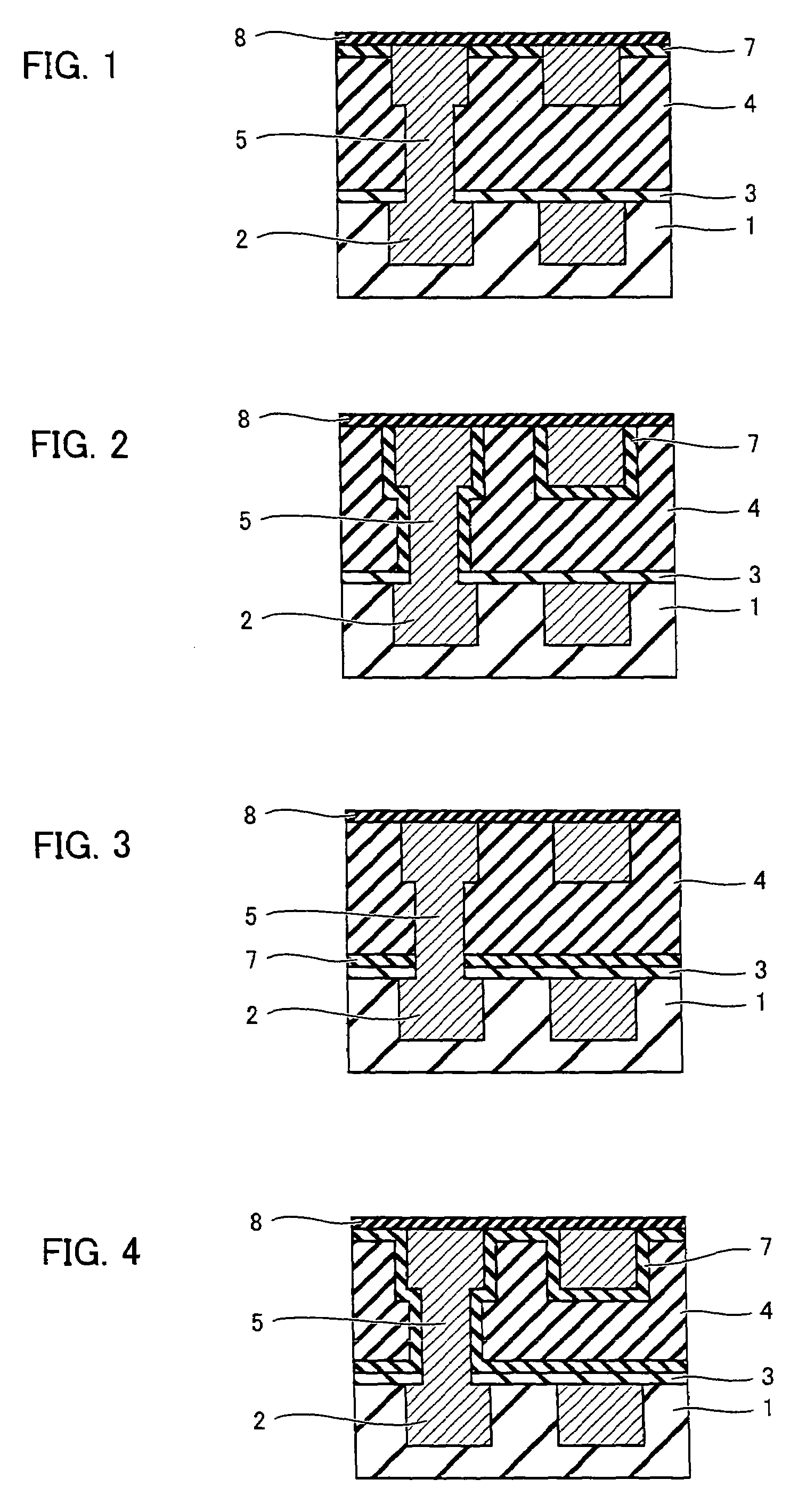
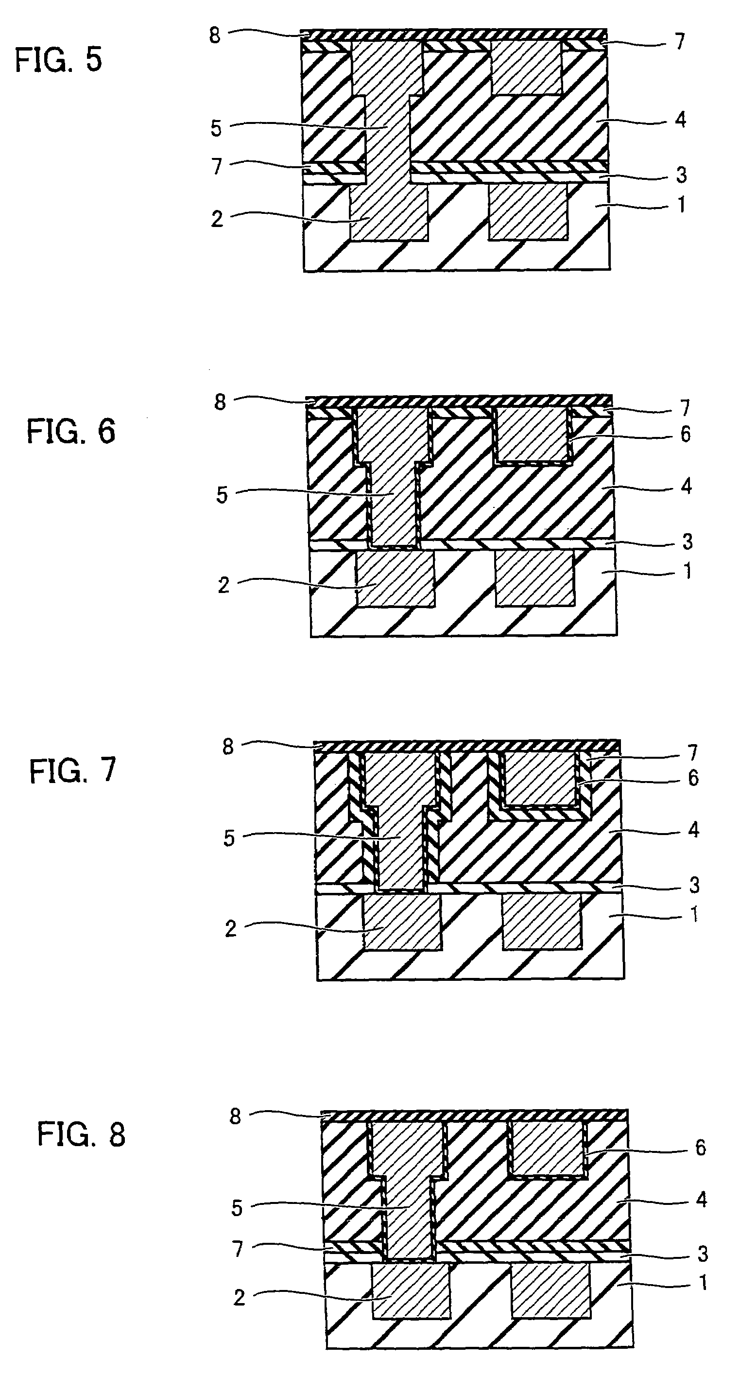
[0027]The present semiconductor device is a semiconductor device including a first insulation layer having a recess with a first conductor layer buried therein, an etching stopper layer formed on the first insulation layer, a second insulation layer formed on the etching stopper layer, a third insulation layer formed on the second insulation layer, and a second conductor layer buried in a recess of the second and third insulation layers. The second and third insulation layers are grown by chemical vapor deposition with a carbon-containing borazine compound used as a source material and the third insulation layer is smaller in carbon content than the second insulation layer.

[0028]The above described, present semiconductor device can have the second and third insulation layers grown by chemical vapor deposition using a carbon-containing borazine compound. The present semiconductor device can thus achieve reduced parasitic capacitance between interconnections, excellent mechanical stre...

second embodiment

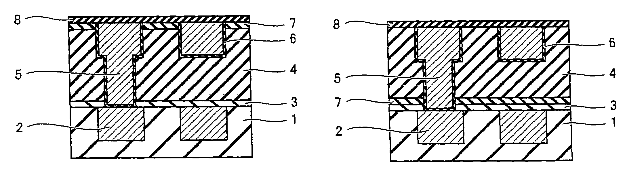
[0051]A semiconductor having a structure shown in FIG. 2 will be described. FIG. 2 is a schematic cross section of a semiconductor device in accordance with the present invention. The semiconductor device of FIG. 2 is identical to that of FIG. 1 except that the former has the second conductor layer 5 having a circumference surrounded by the third insulation layer 7.

[0052]More specifically, the semiconductor device having the structure shown in FIG. 2 includes a first insulation layer 1 having a recess with a first conductor layer 2 buried therein, an etching stopper layer 3 formed on the first insulation layer 1, a second insulation layer 4 formed on etching stopper layer 3, a second conductor layer 5 buried in a recess of the second insulation layer 4, and a third insulation layer 7 formed between the second conductor layer 5 and the second insulation layer 4.

[0053]Herein the second and third insulation layers 4 and 7 are grown by chemical vapor deposition with a carbon-containing ...

third embodiment

[0058]A semiconductor having a structure shown in FIG. 3 will be described. FIG. 3 is a schematic cross section of a semiconductor device in accordance with the present invention. The semiconductor device of FIG. 3 is identical to that of FIG. 1 except that the former has the second conductor layer 5 formed on etching stopper layer 3.

[0059]More specifically, the semiconductor device having the structure shown in FIG. 3 includes a first insulation layer 1 having a recess with a first conductor layer 2 buried therein, an etching stopper layer 3 formed on the first insulation layer 1, a second insulation layer 4 formed on etching stopper layer 3, a third insulation layer 7 formed between the second insulation layer 4 and etching stopper layer 3, and a second conductor layer 5 buried in a recess of the second and third insulation layers 4 and 7.

[0060]Herein the second and third insulation layers 4 and 7 are grown by chemical vapor deposition with a carbon-containing borazine compound us...


PUM


Abstract

There is provided a semiconductor device and method of fabricating the same that employs an insulation film of a borazine-based compound to provided enhanced contact between a material for insulation and that for interconnection, increased mechanical strength, and other improved characteristics. The semiconductor device includes a first insulation layer having a recess with a first conductor layer buried therein, an etching stopper layer formed on the first insulation layer, a second insulation layer formed on the etching stopper layer, a third insulation layer formed on the second insulation layer, and a second conductor layer buried in a recess of the second and third insulation layers. The second and third insulation layers are grown by chemical vapor deposition with a carbon-containing borazine compound used as a source material and the third insulation layer is smaller in carbon content than the second insulation layer.

Description

BACKGROUND OF THE INVENTION[0001]1. Field of the Invention[0002]The present invention relates generally to semiconductor devices and methods of fabricating the same and particularly to semiconductor devices that employ a borazine-based compound for an interlayer insulation film to achieve enhanced contact between the insulation film and an adjacent layer, such as an interconnection layer, a conductor diffusion preventing layer and the like that are adjacent to the insulation film, and methods of fabricating the same.[0003]2. Description of the Background Art[0004]In recent years, as semiconductor integrated circuits are increasingly highly integrated, the circuits have interconnections spaced narrower and increasing in parasitic capacitance therebetween. Semiconductor integrated circuits that require foremost fast operation are required to avoid signal delay and accordingly it is necessary to reduce such parasitic capacitance between interconnections. Furthermore, in order to avoid ...

Claims


Application Information

Patent Timeline
Patent Type & Authority Patents(United States)
IPC IPC(8): H01L23/48
CPCH01L21/314H01L21/76826H01L21/76829H01L21/76835H01L21/76832H01L21/76834H01L21/76831H01L21/02271H01L21/31
Inventor KUMADA, TERUHIKONOBUTOKI, HIDEHARUYASUDA, NAOKIGOTO, KINYAMATSUURA, MASAZUMI
Owner RENESAS ELECTRONICS CORP
Why Eureka
Try Eureka