Method of fabricating flash memory device

a technology of flash memory and memory cells, applied in the direction of semiconductor devices, electrical equipment, basic electric elements, etc., can solve the problems of interfering phenomenon between adjacent memory cells, and degrading a program disturbance characteristi

Inactive Publication Date: 2010-03-23
SK HYNIX INC
View PDF13 Cites 16 Cited by
  • Summary
  • Abstract
  • Description
  • Claims
  • Application Information

AI Technical Summary

Benefits of technology

[0010]The invention can prohibit electrons from migrating from a select transistor to a channel region of a memory cell by forming the select transistors and the memory cells, forming junctions in a semiconductor substrate, and then over etching the semiconductor substrate between the select transistor and an adjacent memory cell using a hard mask pattern.

Problems solved by technology

Thus, an interference phenomenon may occur between adjacent memory cells.
The interference phenomenon is generally generated between adjacent floating gates and may also be generated due to an increased capacitance between the floating gates.
When a program operation in a flash memory device is performed, a program disturbance characteristic may be degraded.
This degrades a program disturbance characteristic.

Method used


Image

  • Method of fabricating flash memory device
  • Method of fabricating flash memory device
  • Method of fabricating flash memory device

Examples


Embodiment Construction

[0019]A specific embodiment according to the invention is described below with reference to the accompanying drawings.

[0020]However, the invention is not limited to the disclosed embodiment, and may be implemented in various other embodiments. The embodiment is provided to complete the disclosure of the invention and to allow those having ordinary skill in the art to understand the scope of the invention. The invention is defined by the appended claims.

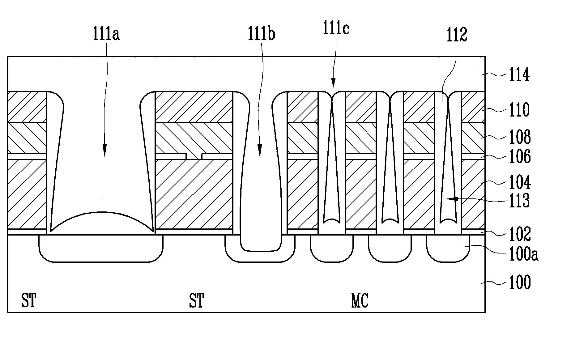
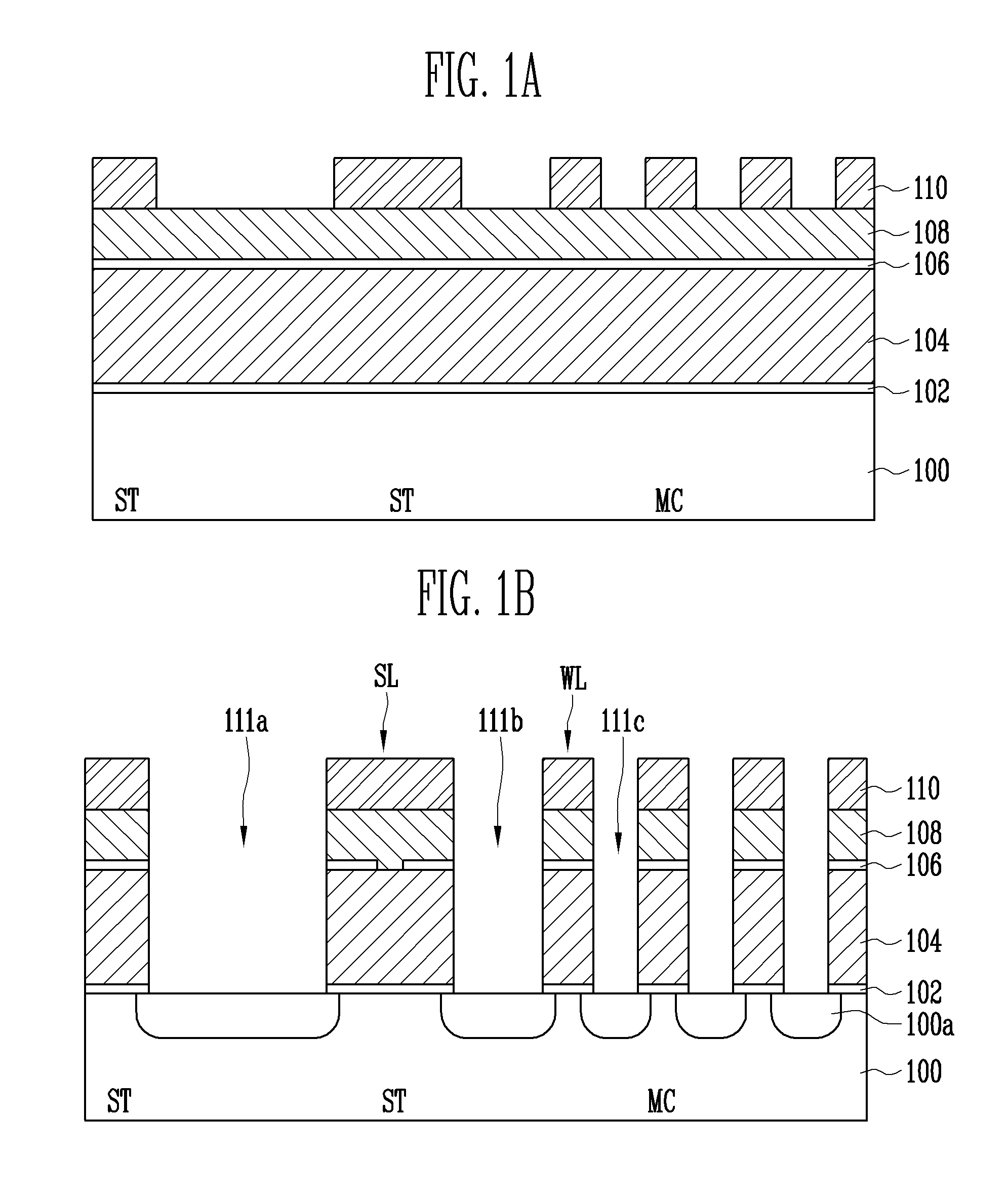
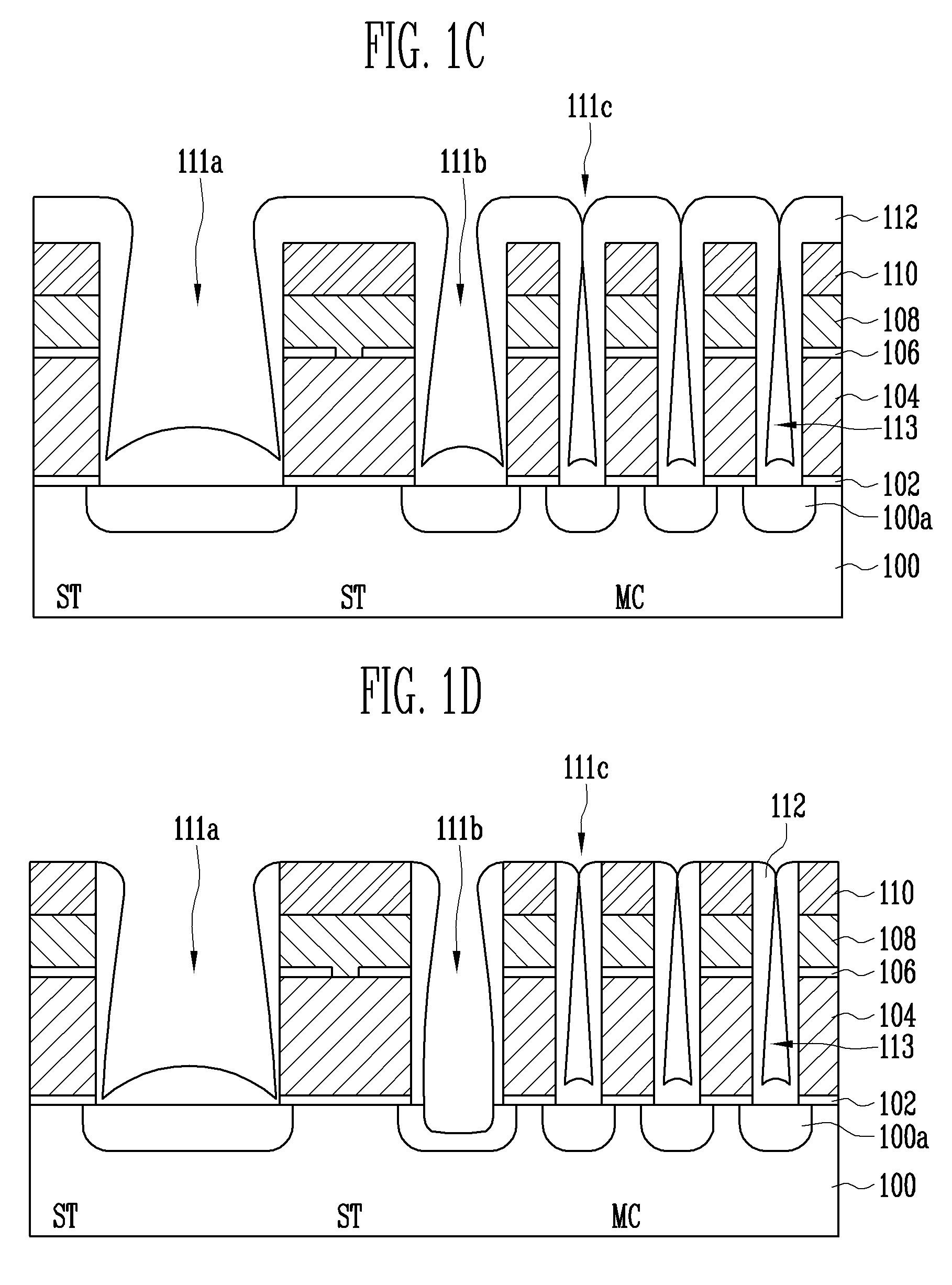
[0021]FIGS. 1A to 1E are sectional views illustrating a method of fabricating a flash memory device according to the invention.

[0022]Referring to FIG. 1A, a first insulating layer 102 for a tunnel insulating film (or a gate insulating layer), a first conductive layer 104 for a floating gate, a dielectric layer 106, and a second conductive layer 108 for a control gate are formed over a semiconductor substrate 100. The first insulating layer 102 may be formed from an oxide layer and the first conductive layer 104 may be formed from a po...


PUM


Abstract

The invention relates to a method of fabricating a flash memory device. According to the method, select transistors and memory cells are formed on, and junctions are formed in a semiconductor substrate. The semiconductor substrate between a select transistor and an adjacent memory cell are over etched using a hard mask pattern. Accordingly, migration of electrons can be prohibited and program disturbance characteristics can be improved. Further, a void is formed between the memory cells. Accordingly, an interference phenomenon between the memory cells can be reduced and, therefore, the reliability of a flash memory device can be improved.

Description

CROSS-REFERENCE TO RELATED APPLICATION[0001]Priority to Korean patent application number 10-2007-64533, filed on Jun. 28, 2007, which is incorporated by reference in its entirety, is claimed.BACKGROUND OF THE INVENTION[0002]The invention relates to a method of fabricating a flash memory device and, more particularly, to a method of fabricating a flash memory device that reduces disturbance between gates.[0003]A flash memory device includes a cell region including a memory cell, and a peripheral (“peri”) region including transistors for transferring a driving voltage. The cell region is described in detail below.[0004]The cell region comprises strings having a plurality of memory cells connected in series. Each string includes a plurality of memory cells and a select transistor formed at both ends of the string. The memory cell has a structure in which a tunnel insulating film, a floating gate, a dielectric layer, and a control gate are sequentially laminated over a semiconductor sub...

Claims


Application Information

Patent Timeline
Patent Type & Authority Patents(United States)
IPC IPC(8): H01L21/336
CPCH01L27/11521H01L27/11524H10B41/35H10B41/30H01L21/31051H01L21/67069H10B63/30
Inventor KIM, EUN SOOCHO, WHEE WONHONG, SEUNG HEE
Owner SK HYNIX INC
Why Eureka
Try Eureka