Method of manufacturing flash memory device

a technology of flash memory and manufacturing method, which is applied in the direction of semiconductor devices, basic electric elements, electrical appliances, etc., can solve the problems of affecting the integration of semiconductor devices, affecting the stability of the device, and the interference phenomenon between neighboring cells becomes the most important problem, so as to achieve the effect of reducing the interference phenomenon between neighboring cells and increasing the degree of integration

Active Publication Date: 2007-07-12
SK HYNIX INC
View PDF11 Cites 13 Cited by
  • Summary
  • Abstract
  • Description
  • Claims
  • Application Information

AI Technical Summary

Benefits of technology

[0009]In one embodiment, the invention provides a method of manufacturing a flash memory device, in which a floating gate can be formed using one conductive layer without using the SA-STI process having a limit as the degree of integration of semiconductor devices is increased and an interference phenomenon between neighboring cells can be minimized by securing a sufficient distance between the cells.

Problems solved by technology

As a result, the interference phenomenon between the neighboring cells whose states are changed becomes the most important problem.
Accordingly, the distributions of the threshold voltage of the program cell are widely changed, resulting in failure of a chip.
The interference problem between neighboring cells becomes more profound in multi-level cells.
However, as the level of integration of devices is increased, to secure a sufficient distance between the cells has a limit.
As a result, the process employing the floating gate mask is no longer used.

Method used


Image

  • Method of manufacturing flash memory device
  • Method of manufacturing flash memory device
  • Method of manufacturing flash memory device

Examples


first embodiment

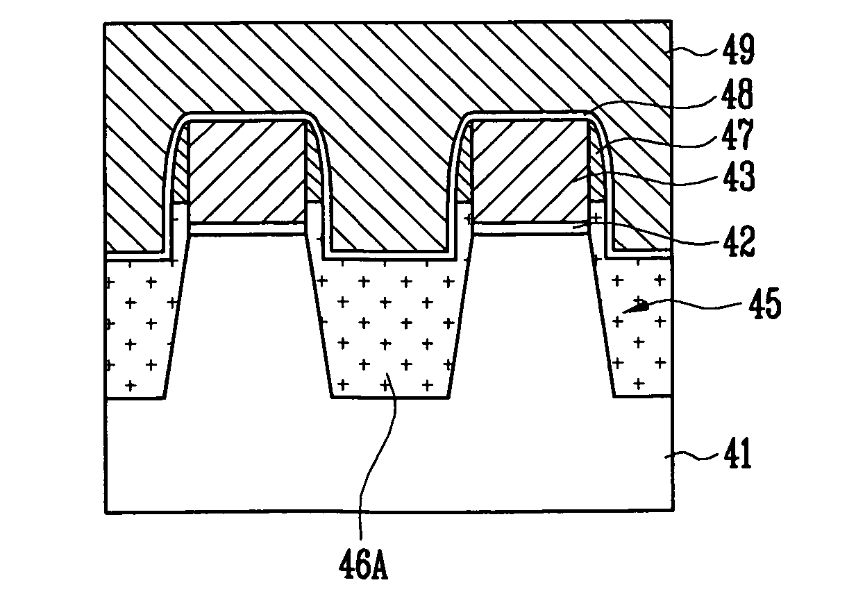
[0032]FIGS. 1A to 1D are cross-sectional views illustrating a method of manufacturing a flash memory device according to the invention.

[0033]Referring to FIG. 1A, a tunnel oxide film 12, a first conductive layer 13, and a hard mask film 14 are sequentially formed on a semiconductor substrate 11. The first conductive layer 13 may preferably be formed to a thickness of 700 Å to 1500 Å by laminating an undoped polysilicon film and a doped polysilicon film in order to prevent warping of the tunnel oxide film 12. The undoped polysilicon film may be formed to have a thickness, which is half or less a total thickness of the first conductive layer 13. Meanwhile, the first conductive layer 13 may preferably be formed to a thickness of 1000 Å to 1500 Å when it is applied to single level cells and may preferably be formed to a thickness of 700 Å to 1000 Å when it is applied to multi-level cells. Furthermore, the hard mask film 14 may be formed using a nitride film.

[0034]The hard mask film 14 i...

second embodiment

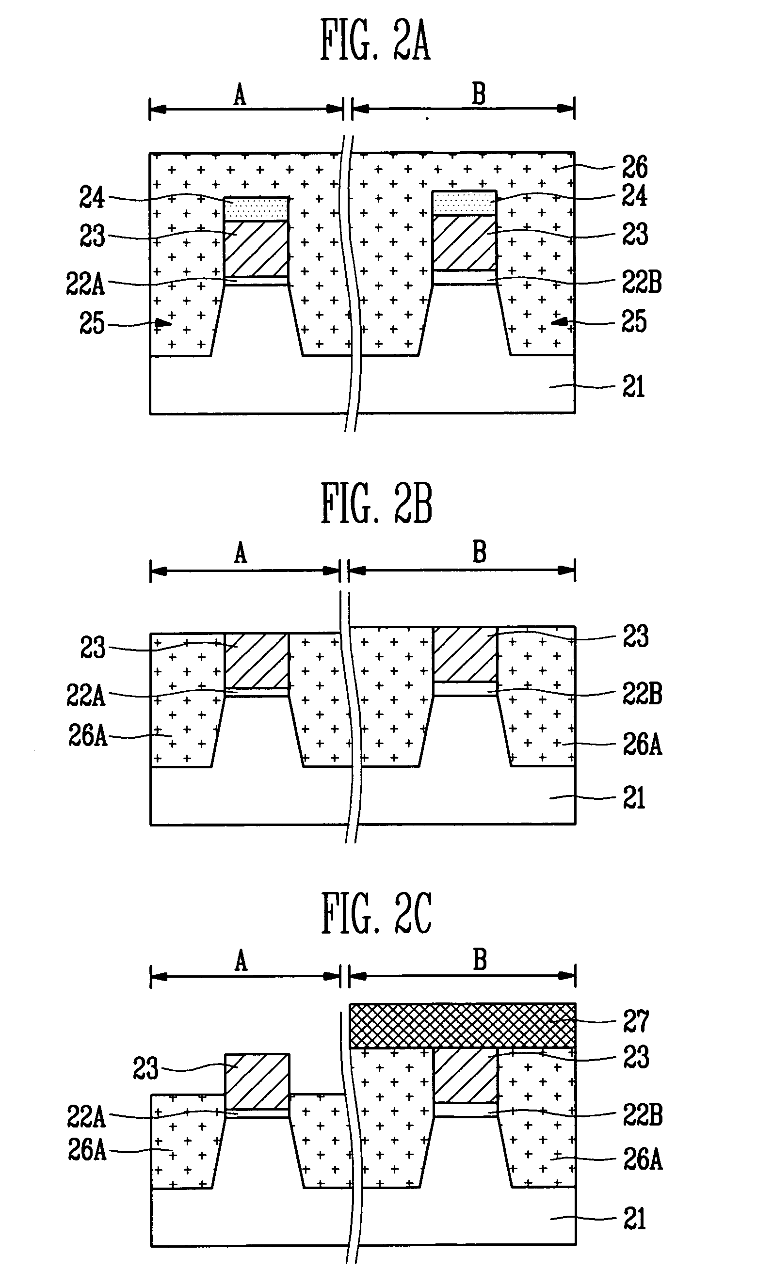
[0040]FIGS. 2A to 2E are cross-sectional views illustrating a method of manufacturing a flash memory device according to the invention.

[0041]Referring to FIG. 2A, there is provided a semiconductor substrate 21 in which a cell region A, a high-voltage transistor region B, and the like are defined. A tunnel oxide film 22A is formed on the semiconductor substrate 21 of the cell region A. A gate oxide film 22B having a thickness thicker than that of the tunnel oxide film 22A is formed on the semiconductor substrate 21 of the high-voltage transistor region B. The tunnel oxide film 22A may preferably be formed to a thickness of 70 Å to 90 Å and the gate oxide film 22B may preferably be formed to a thickness of 350 Å to 400 Å.

[0042]A first conductive layer 23 and a hard mask film are formed on the entire structure 24. The first conductive layer 23 may preferably be formed to a thickness of 700 Å to 1400 Å by laminating an undoped polysilicon film and a doped polysilicon film. The undoped p...

third embodiment

[0048]FIGS. 3A to 3E are cross-sectional views illustrating a method of manufacturing a flash memory device according to the invention.

[0049]Referring to FIG. 3A, there is provided a semiconductor substrate 31 in which a cell region A and a high-voltage transistor region B are defined. The semiconductor substrate 31 of the high-voltage transistor region B is etched at a predetermined depth. In this case, the etch depth of the semiconductor substrate 31 is decided taking a thickness of a tunnel oxide film formed in the cell region A and a thickness of a gate oxide film formed in the high-voltage transistor region B into consideration. For example, in the case where the tunnel oxide film is preferably formed to a thickness of 70 Å to 90 Å in the cell region A and the gate oxide film is preferably formed to a thickness of 350 Å to 400 Å in the high-voltage transistor region, the semiconductor substrate 31 may be etched to a depth of 260 Å to 330 Å, for example.

[0050]Referring to FIG. 3...


PUM


Abstract

A method of manufacturing a flash memory device. According to the invention, a floating gate can be formed and a distance between cells can be secured sufficiently by using one conductive layer without using a SA-STI process that cannot be applied to the manufacture process of high-integrated semiconductor devices. It is therefore possible to minimize an interference phenomenon between neighboring cells. Furthermore, an isolation film is etched after a photoresist film covering only a high-voltage transistor region is formed, or a gate oxide film is formed after a semiconductor substrate is etched at a thickness, which is the same as that of the gate oxide film of the high-voltage transistor region, so that a step between the cell region and the high-voltage transistor region is the same. Accordingly, the coupling ratio can be increased even by the gate oxide film of the high-voltage transistor region, which is thicker than the tunnel oxide film of the cell region. In addition, damage to a tunnel oxide film, a semiconductor substrate or a floating gate while an isolation film is etched at a predetermined depth in order to control the EFH can be prevented by controlling the EFH in such a manner than conductive layer spacers are formed on sidewalls of the floating gate and the isolation film is further etched.

Description

BACKGROUND[0001]1. Field of the Invention[0002]The invention relates generally relates to semiconductor memory devices and, more particularly, to a method of manufacturing a flash memory device, in which an interference phenomenon between neighboring cells in high-integrated semiconductor devices can be minimized and the coupling ratio can be enhanced by controlling the effective field height (EFH) by etching an isolation film at a predetermined thickness.[0003]2. Discussion of Related Art[0004]A NAND flash memory device performs data program by injecting electrons into the floating gate by Fowler-Nordheim (FN) tunneling phenomenon, thereby proving a large capacity and a high degree of integration.[0005]The NAND flash memory device includes a plurality of cell blocks. One cell block includes a plurality of cell strings in which a plurality of cells for storing data are in series connected to form one string, and a drain select transistor and a source select transistor formed between...

Claims


Application Information

Patent Timeline
Patent Type & Authority Applications(United States)
IPC IPC(8): H01L21/336
CPCH01L27/105H01L27/115H01L27/11541H01L27/11526H01L27/11536H01L27/11521H10B69/00H10B41/30H10B41/44H10B41/47H10B41/40
Inventor HWANG, JOO WONPARK, BYUNG SOOLEE, GA HEE
Owner SK HYNIX INC
Why Eureka
Try Eureka