
Semiconductor device using magnetic domain wall movement

a magnetic domain wall and magnetic field technology, applied in the field can solve the problems of reducing reliability, slow reading and writing speed, flash memory drawbacks, etc., and achieve the effect of improving the speed of magnetic domain wall movement and reading/writing speed

Active Publication Date: 2010-03-23
SAMSUNG ELECTRONICS CO LTD
View PDF5 Cites 4 Cited by
  • Summary
  • Abstract
  • Description
  • Claims
  • Application Information

AI Technical Summary

Benefits of technology

The present invention provides a semiconductor device that uses magnetic domain wall movement to increase reading / writing speeds by improving the speed of movement of magnetic domain walls. The device includes a magnetic substance film in which magnetic domain walls are moved. The film has a damping constant of at least 0.015, which indicates its ability to control the movement of magnetic domain walls. The film may be an alloy containing a non-magnetic substance, such as osmium, ruthenium, or silver, in a magnetic substance like nickel or iron. The non-magnetic substance may be present in the film in an amount of 0.5 to 10 atom%. The device may also include a non-magnetic seed layer or a non-magnetic capping layer on the magnetic substance film to further enhance its performance.

Problems solved by technology

However, a device that has a rotating part like the HDD has a problem in that it wears down over time, and thus, there is a high possibility of operational failure, thereby reducing reliability.
However, the flash memory has drawbacks of slow reading and writing speeds and short life span.
However, the flash memory, FRAM, MRAM, and PRAM all have small storage capacities when compared to a HDD and have high manufacturing costs.
However, the development of semiconductor devices that use the magnetic domain wall movement is still in an initial stage, and there are a few problems that have yet to be solved in order for them to be used in practice.
One of the problems is related to the mobility of the magnetic domain walls.
If the movement of the magnetic domain walls is slow, a sufficient speed of reading / writing cannot be achieved.
However, a physical phenomenon in relation to the speed of movement of the magnetic domain walls has not yet been theoretically clearly identified.
Therefore, there is a difficulty in improving the speed of movement of the magnetic domain walls.

Method used


Image

  • Semiconductor device using magnetic domain wall movement
  • Semiconductor device using magnetic domain wall movement
  • Semiconductor device using magnetic domain wall movement

Examples


Embodiment Construction

[0032]A semiconductor device that uses magnetic domain wall movement according to an exemplary embodiment of the present invention will now be described more fully with reference to the accompanying drawings.

[0033]First, a theoretical principle of the present invention will be described.

[0034]In order to investigate the movement phenomenon of magnetic domain walls within a magnetic field, the following experiments were conducted. Through the experiments, the causes of interference with the movement of the magnetic domain walls and a method of improving the speed of movement of the magnetic domain walls were found.

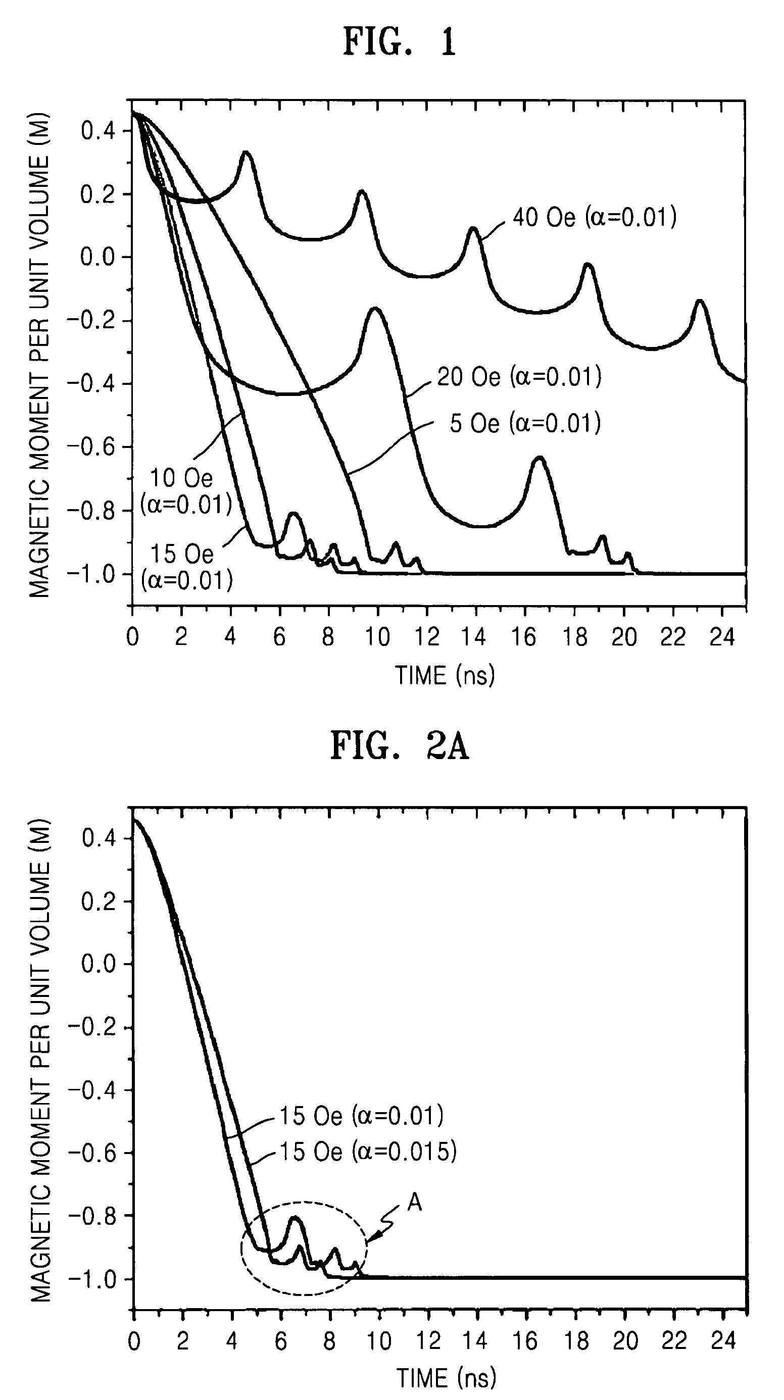
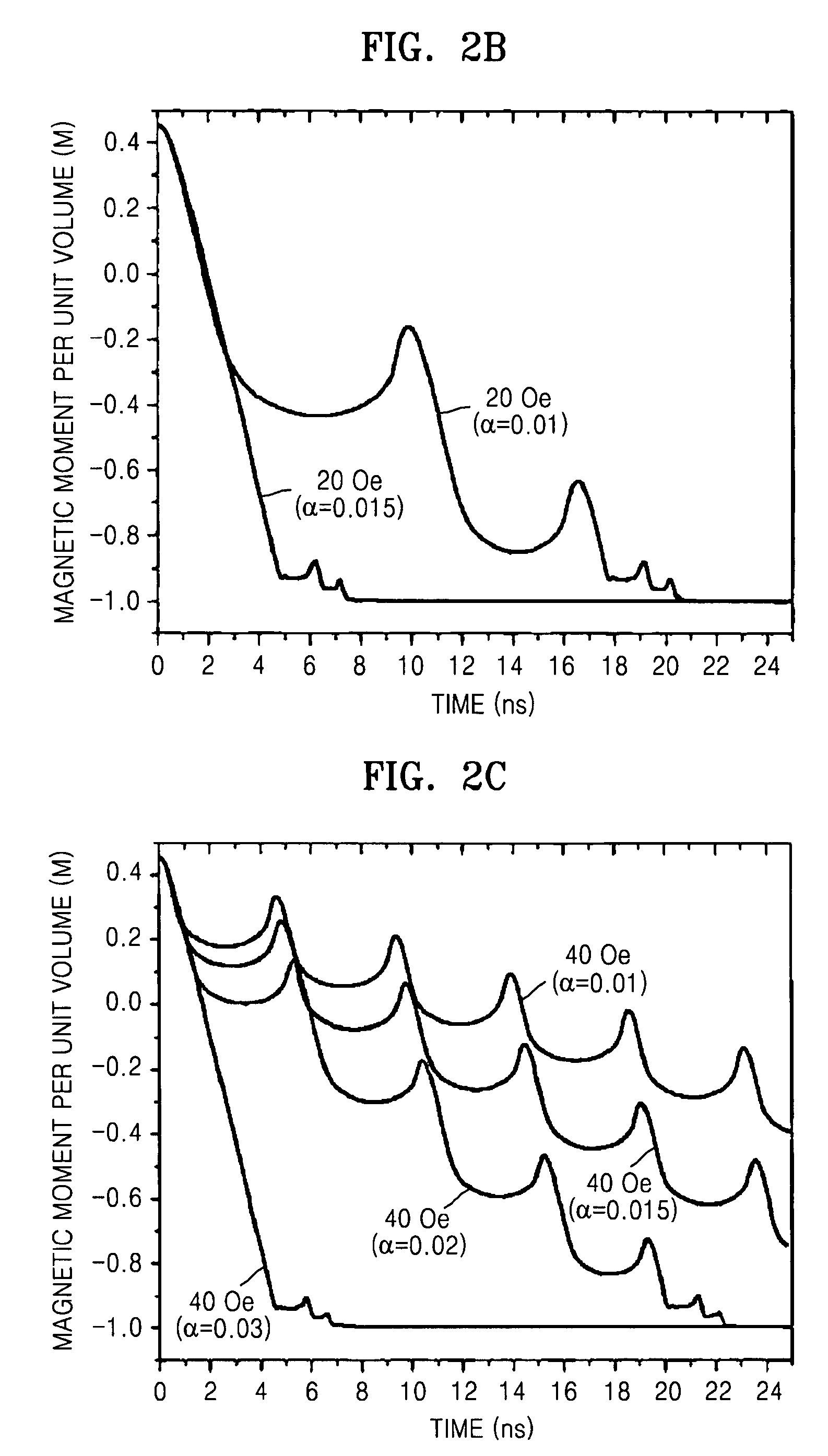
[0035]First, the movement phenomenon of magnetic domain walls in five magnetic substance samples having an identical damping constant and each having two magnetic domains in different directions from each other was examined by applying magnetic fields that were different from each other. The results are shown in FIG. 1. At this time, each of the magnetic substance samples i...


PUM


Abstract

A semiconductor device to which magnetic domain wall movement is applied is provided. The semiconductor device includes a magnetic substance film in which magnetic domain walls are moved, and the magnetic substance film has a damping constant of 0.015 to 0.1.

Description

CROSS-REFERENCE TO RELATED PATENT APPLICATIONS[0001]This application claims priority from Korean Patent Application No. 10-2006-0065863, filed on Jul. 13, 2006, in the Korean Intellectual Property Office, the disclosure of which is incorporated herein in its entirety by reference.BACKGROUND OF THE INVENTION[0002]1. Field of the Invention[0003]The present invention relates to a semiconductor device and, more particularly, to a semiconductor device to which magnetic domain wall movement is applied.[0004]2. Description of the Related Art[0005]Data storing devices are divided, for the most part, into volatile data storing devices that lose all recorded data when power is turned off and non-volatile data storing devices that keep data even when power is turned off.[0006]Non-volatile data storing devices include a hard disc drive (HDD) and a non-volatile random access memory (RAM). The HDD includes a read and write head and a rotating data recording medium, and can store data of 100 gigab...

Claims


Application Information

Patent Timeline
Patent Type & Authority Patents(United States)
IPC IPC(8): G11C11/14
CPCG11B5/65G11B5/72G11B5/732G11C19/0808H01F10/14H01F10/16Y10S977/933G11B5/7379Y10T428/31504Y10T428/31678G11B5/657G11C11/15H10B99/00
Inventor LIM, CHEE-KHENGKIM, EUN-SIKLEE, SUNG-CHUL
Owner SAMSUNG ELECTRONICS CO LTD
Learn More