Semiconductor memory and system with matching characteristics of signal supplied to a dummy signal line and a real signal line

a technology of dummy signal and memory, applied in the field of semiconductor memory, can solve the problems of reducing yield, disconnection failure, and inability to fully perform the test on a real signal line adjacent to the dummy signal lin

Inactive Publication Date: 2010-04-13
SOCIONEXT INC
View PDF14 Cites 11 Cited by
  • Summary
  • Abstract
  • Description
  • Claims
  • Application Information

AI Technical Summary

Problems solved by technology

The difference in shape may cause a short failure and a disconnection failure, which becomes a factor behind a reduction in yield.
This causes a problem that a test on a real signal line adjacent to the dummy signal line cannot be fully performed.
More specifically, for example, in the real signal line adjacent to the dummy signal line, the influence of a coupling capacitance between the adjacent signal lines cannot be fully evaluated.
Moreover, as described above, since the driving timing of the dummy signal line is different from that of the real signal line, so that the dummy signal line cannot be used as the real signal line.

Method used


Image

  • Semiconductor memory and system with matching characteristics of signal supplied to a dummy signal line and a real signal line
  • Semiconductor memory and system with matching characteristics of signal supplied to a dummy signal line and a real signal line
  • Semiconductor memory and system with matching characteristics of signal supplied to a dummy signal line and a real signal line

Examples


first embodiment

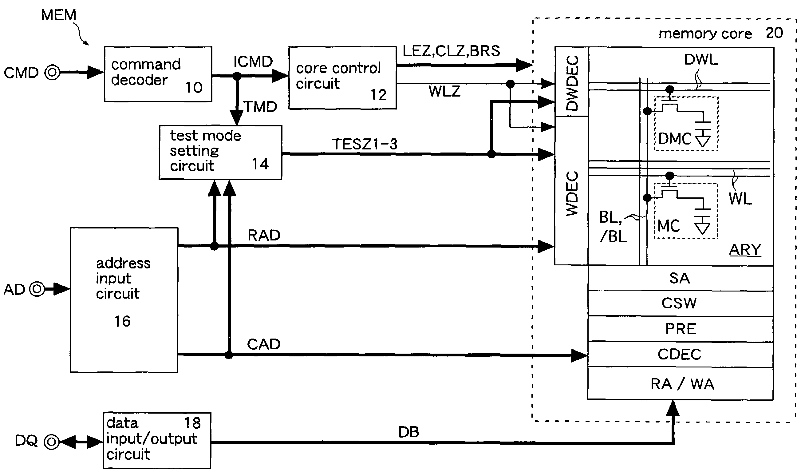
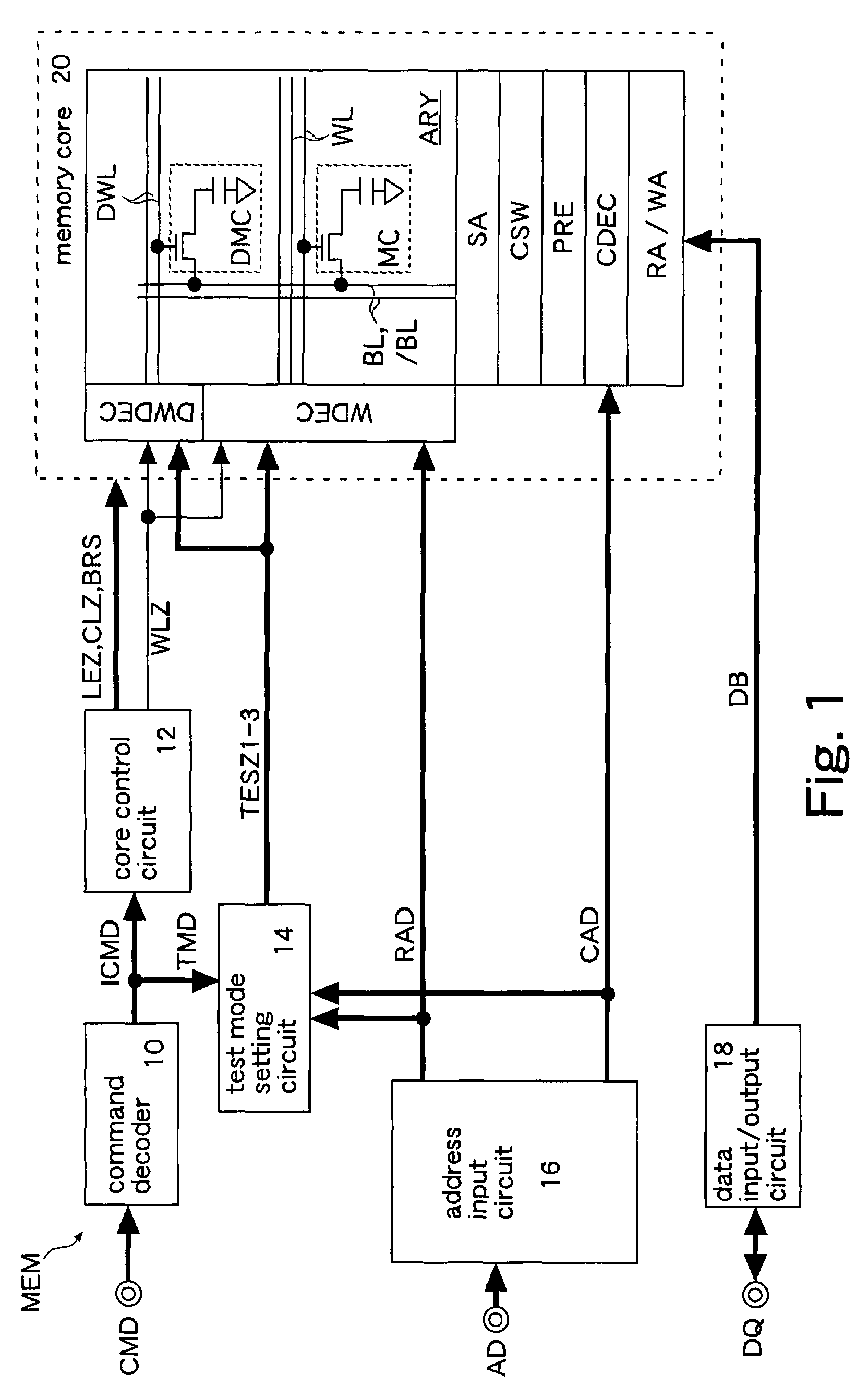
[0042]FIG. 1 shows the present invention. A semiconductor memory MEM is, for example, an FCRAM (Fast Cycle RAM). The FCRAM is a pseudo SRAM including DRAM memory cells and including an SRAM interface. The memory MEM includes a command decoder 10, a core control circuit 12, a test mode setting circuit 14, an address input circuit 16, a data input / output circuit 18, and a memory core 20. Further, to automatically perform a refresh operation of a memory cell MC, the semiconductor memory MEM includes a refresh timer to generate an internal refresh request, a refresh address counter to generate a refresh address, and so on (not shown). Since the present invention does not relate to control of the refresh operation, circuits and operations related to the refresh operation will not be described.

[0043]The command decoder 10 outputs an internal command signal ICMD (read command, write command), a test mode command TMD, and so on in response to a command signal CMD (for example, a chip enable...

second embodiment

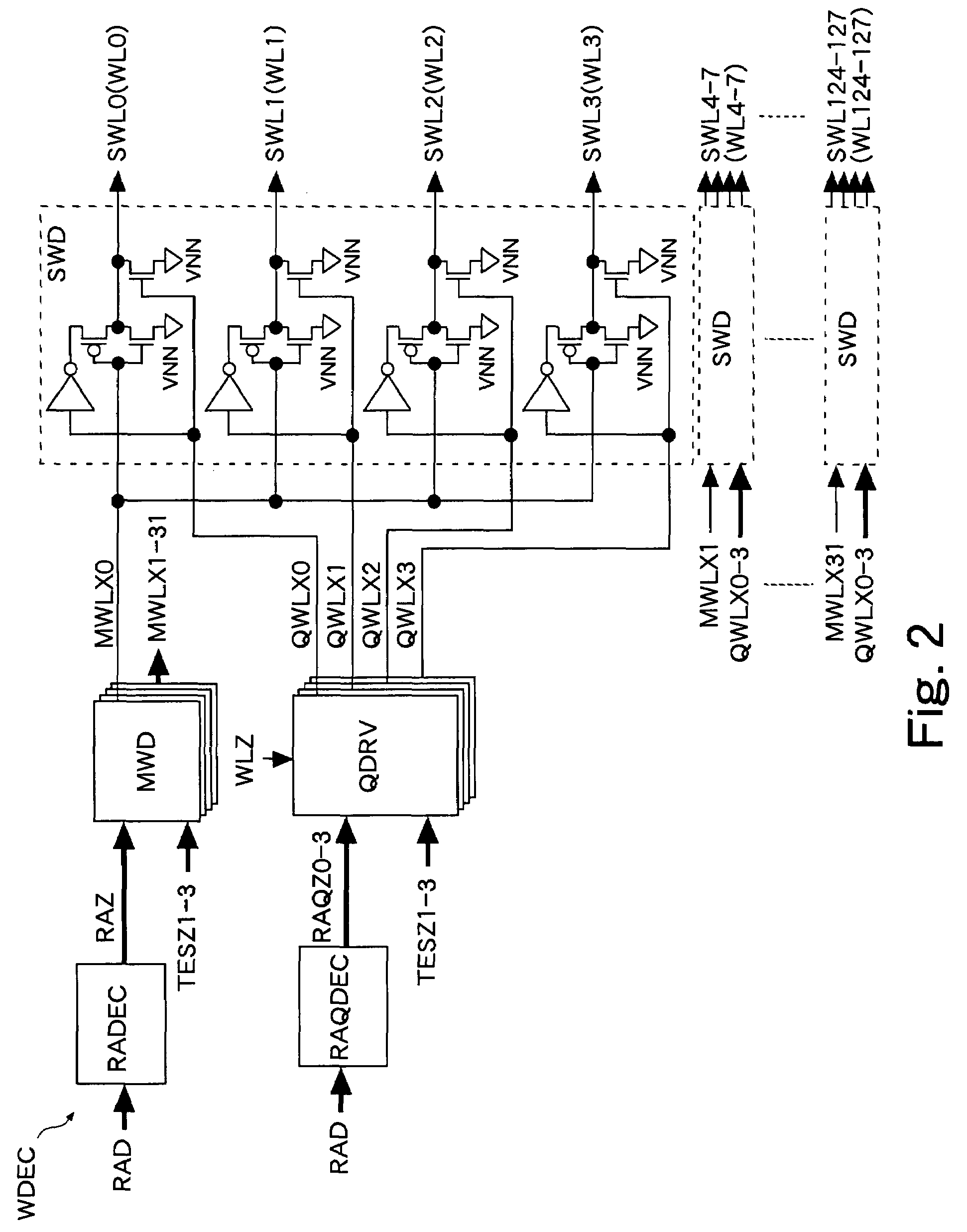
[0056]FIG. 3 shows details of the dummy word decoder DWDEC shown in FIG. 1. A detailed description of circuits having the same configurations as those of the word decoder WDEC shown in FIG. 2 is omitted. The dummy word decoder DWDEC includes dummy main word decoders DMWD and dummy sub-word decoders DSWD. The dummy main word decoder DMWD has the same circuit configuration as the real main word decoder MWD shown in FIG. 2 except that a terminal receiving a dummy decode signal DRAZ is connected to a power supply line VII. The dummy sub-word decoder DSWD has the same circuit configuration as the real sub-word decoder SWD and receives the real sub-word activation signals QWLX0-3. Incidentally, as will be described in a second embodiment and so on discussed later, the dummy decode signal DRAZ is used when data is inputted / outputted to / from the dummy memory cell MC.

[0057]The dummy main word decoders DMWD activate the dummy main word lines DMWLX (DMWLX0-1) to a low logic level in response t...

sixth embodiment

[0116]FIG. 20 shows an operation of the memory MEM in the test mode of the In this embodiment, by the setting of the test mode setting circuit 14E, the operation mode is shifted from the normal operation mode to the test mode, and only the test control signal TESZ5 is activated to a high logic level. The memory MEM performs a fifth stress test, for example, in response to the access command from the memory control unit MCNT shown in FIG. 6 or FIG. 7.

[0117]In response to the access command (write command, for example), the precharge control signal BRS is inactivated to a low logic level, and the word line WL is activated. The number of word lines WL to be activated may be one which corresponds to the row address RAD, or all of the word lines WL may be activated. Incidentally, when no stress is given to the memory cells MC and DMC, the word line WL may not be activated. In this case, by supplying the test mode command TMD to start / end the test to the core control circuit 12E, the sen...


PUM


Abstract

To fully evaluate a real signal line and a real memory cell adjacent to a dummy signal line and utilize dummy signal line as real signal line, a semiconductor memory includes at least one real signal line connected to real memory cells driven by a real driver and at least one dummy signal line outside the real signal line connected to dummy memory cells, driven by a dummy driver. Real driver and dummy driver drive the real signal line and the dummy signal line synchronous with a common timing signal generated by an operation control circuit. Consequently, a stress evaluation is also performable, e.g., on a real signal line outside of a memory cell array under the same condition of a real signal line on the inner side. Dummy signal line is driven using common timing signal and evaluated, thus being usable as a redundancy signal line to relieve failure.

Description

CROSS REFERENCE TO RELATED APPLICATION[0001]This application is based upon and claims the benefit of priority from Japanese Patent Application No. 2006-222548, filed on Aug. 17, 2006, the entire contents of which are incorporated herein by reference.BACKGROUND[0002]1. Field[0003]The present invention relates to a semiconductor memory including a dummy circuit of dummy memory cells and so on.[0004]2. Description of the Related Art[0005]In a memory cell array of a semiconductor memory, elements and wirings are formed with higher density, compared to peripheral circuits. Therefore, in a manufacturing process of the semiconductor memory, the shapes of the elements and wirings in an inner portion of the memory cell array sometimes differ from those in an outer peripheral portion due to the influence of halation or the like. The difference in shape may cause a short failure and a disconnection failure, which becomes a factor behind a reduction in yield.[0006]Conventionally, in order to ma...

Claims


Application Information

Patent Timeline
Patent Type & Authority Patents(United States)
IPC IPC(8): G11C29/00
CPCG11C29/838G11C29/24G11C11/401G11C2029/1202G11C7/00
Inventor KOBAYASHI, HIROYUKI
Owner SOCIONEXT INC
Why Eureka
Try Eureka