Method and apparatus for routing efficient built-in self test for on-chip circuit blocks

a built-in self test and circuit block technology, applied in the direction of electronic circuit testing, measurement devices, instruments, etc., can solve the problems of increasing the difficulty of cost effective testing of memory blocks, increasing the cost of having separate on-chip bist controllers for each memory block, and increasing the demand on the interconnect structure of the pld, so as to avoid the high routing congestion

Inactive Publication Date: 2010-04-27
ALTERA CORP
View PDF52 Cites 17 Cited by
  • Summary
  • Abstract
  • Description
  • Claims
  • Application Information

AI Technical Summary

Benefits of technology

[0014]The present invention includes built-in self test techniques for testing on-chip circuit blocks (e.g., memory blocks) on integrated circuits. A reduced number of BIST controllers are provided on-chip to test numerous circuit blocks. The present invention avoids the high routing congestion by utilizing scan chain segments that run continuously along the inputs and outputs of the circuit blocks. The BIST controller takes control of the scan chains during memory test and has the ability to partition the scan chains at specified intervals.

Problems solved by technology

As the number of on-chip memory blocks in PLDs increases, it becomes increasingly difficult to test the memory blocks in a cost effective manner.
As a result, it is not cost effective to have separate on-chip BIST controllers for each memory block.
However, this techniques places a large demand on the PLD's interconnect structure.
Soft BIST controllers cannot be programmed into MPLDs to test on-chip memory blocks, because the functionality of the on-chip logic is fixed during manufacture.
However, it is very expensive in terms of tester time and memory to run all the memory vectors from the tester.
Also, getting enough pins to access all the memory blocks may be difficult to come by.
It is not cost effective to have an individual BIST controller for every memory block on an integrated circuit (IC) that has a large number of small memory blocks.
On other hand, using one BIST controller that routes test signals directly it to hundreds of memory blocks all over an IC along dedicated routing wires causes routing congestion.

Method used


Image

  • Method and apparatus for routing efficient built-in self test for on-chip circuit blocks
  • Method and apparatus for routing efficient built-in self test for on-chip circuit blocks
  • Method and apparatus for routing efficient built-in self test for on-chip circuit blocks

Examples


Embodiment Construction

[0022]The techniques of the present invention can be used to test circuits blocks on an integrated circuit such as a mask programmable logic device (MPLD) or an application specification integrated circuit (ASIC). Memory blocks are one example of circuit blocks that can be tested according to the techniques of the present invention. The present invention can also be used to test other types of circuit blocks such as digital signal processing (DPS) blocks.

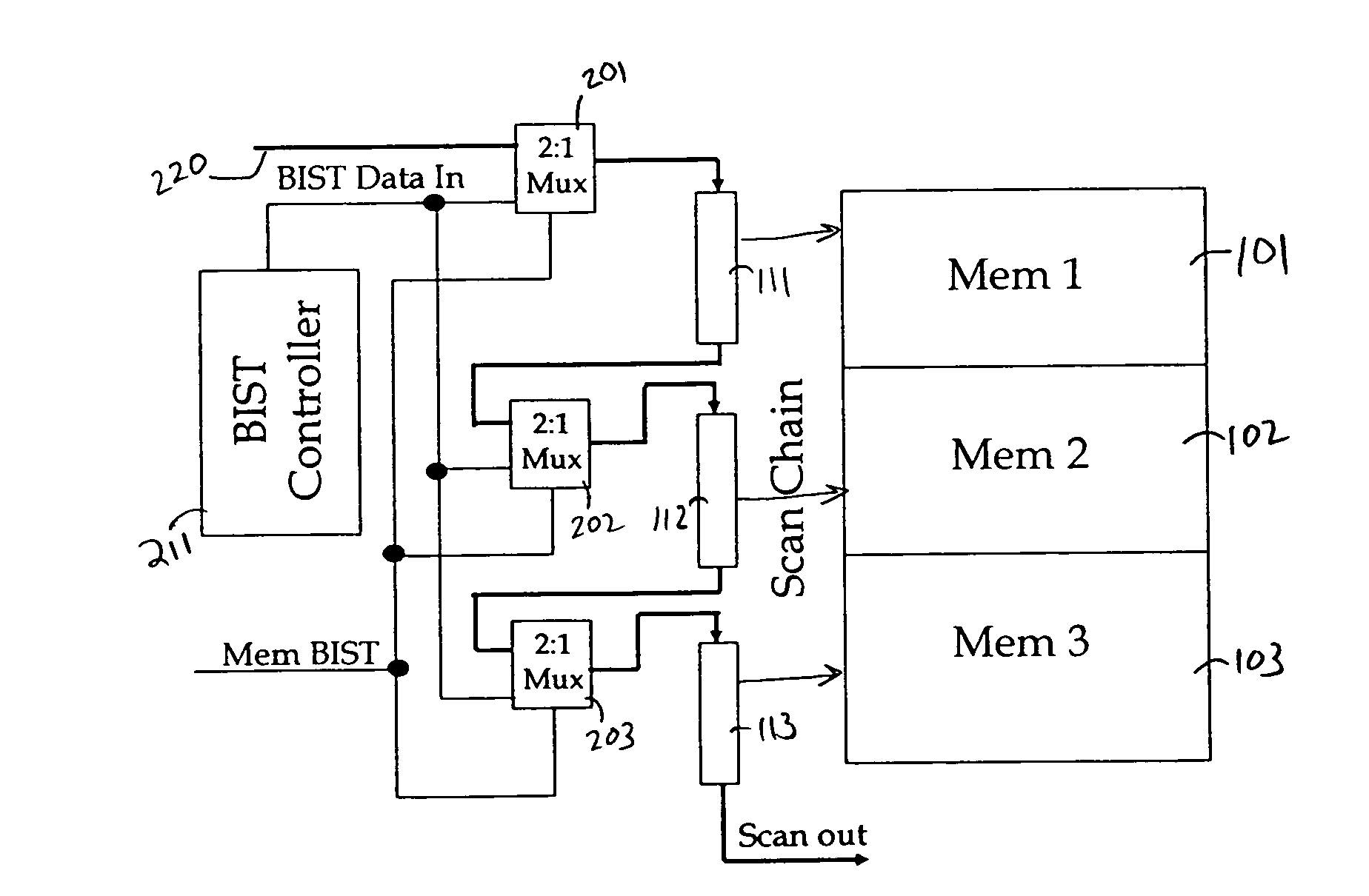
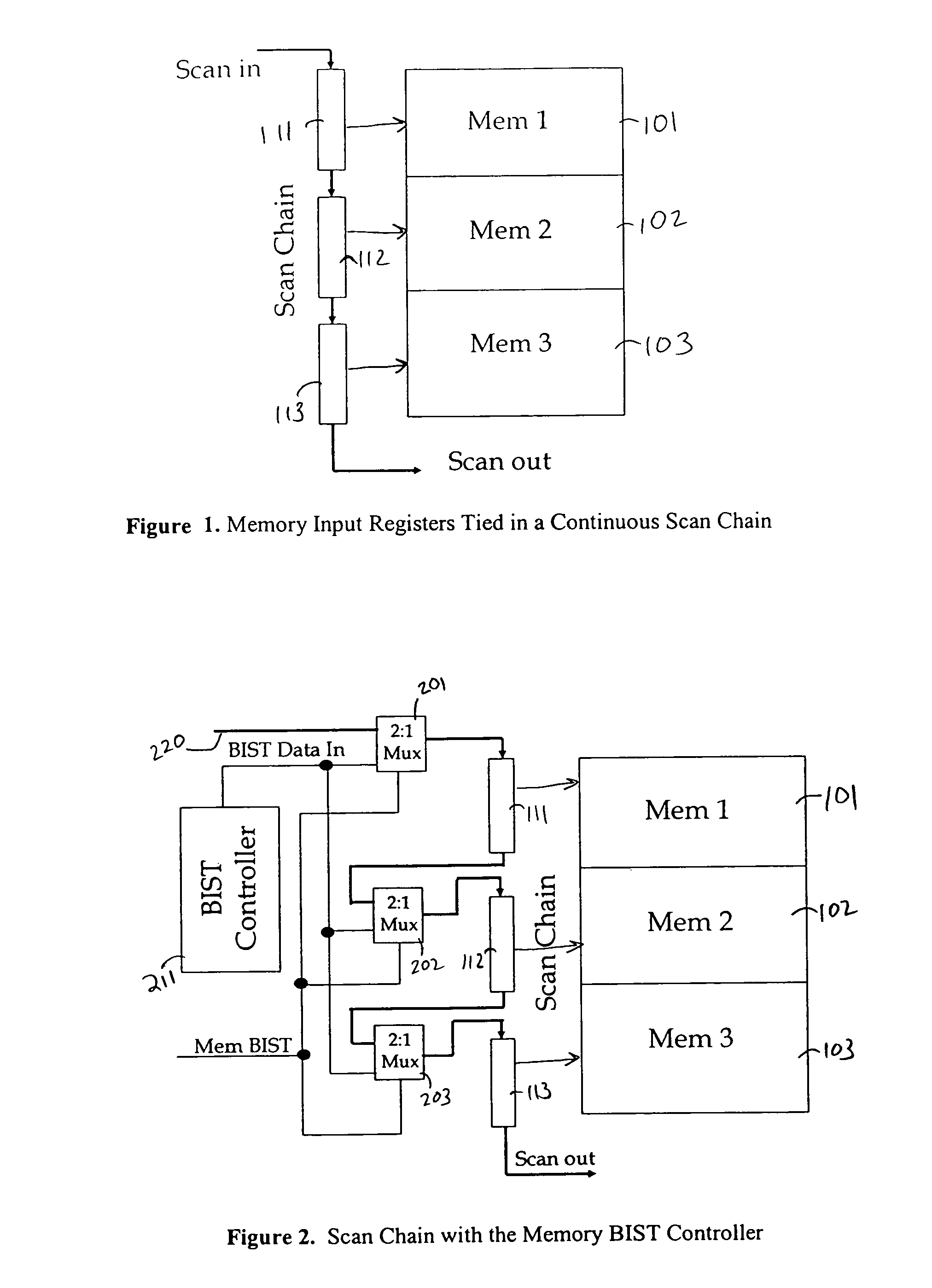
[0023]FIG. 1 shows a typical example of three contiguous memory blocks 101, 102, and 103 on an integrated circuit (IC). A memory block on a MPLD or other type of IC typically has input and output registers that are used to store data bits transferred to and from the memory block.

[0024]Memory blocks 101-103 receive data from input registers 111, 112, and 113, respectively. Input registers 111-113 can be serially coupled together as scan chain segments of shift registers as shown in FIG. 1. Alternatively, shadow registers can be place...


PUM


Abstract

Built-in self test techniques for testing circuit blocks on integrated circuits are provided. A BIST controller is provided on-chip to test two or more circuit blocks. High routing congestion is avoided by loading test data into the circuit blocks through scan chain segments that run continuously along the inputs and outputs of the circuit blocks. The BIST controller takes control of the scan chain segments during test and has the ability to partition the scan chains at specified intervals.

Description

BACKGROUND OF THE INVENTION[0001]The present invention relates to built-in self tests for on-chip circuit blocks, and more particularly, to configurations for built-in self tests for on-chip circuit blocks that reduce routing and die area.[0002]Programmable logic devices (PLDs) are integrated circuits that can be configured to perform a variety of user functions. PLDs typically have numerous logic blocks that can be configured to implement various combinatorial and sequential functions. The logic blocks have access to a programmable interconnect structure. The programmable interconnect structure can be programmed to interconnect the logic blocks in almost any desired configuration.[0003]PLDs usually have on-chip memory blocks. Each of the memory blocks contains an array of memory cells. The memory cells can be, for example, SRAM, DRAM, EPROM, EEPROM, or Flash EEPROM cells. The memory blocks are dispersed throughout the chip in between the logic blocks.[0004]After a PLD is manufactur...

Claims


Application Information

Patent Timeline
Patent Type & Authority Patents(United States)
IPC IPC(8): G01R31/28G11C29/00
CPCG11C29/16G11C29/32G11C29/26G11C2029/3202
Inventor DASTIDAR, JAYABRATA GHOSH
Owner ALTERA CORP
Why Eureka
Try Eureka