Semiconductor packages and methods of fabricating the same

a technology of semiconductors and packages, applied in the direction of semiconductor/solid-state device details, semiconductor devices, electrical apparatus, etc., can solve the problems of difficult insulate the die pad from external air, large amount of heat generated by the semiconductor chip, and difficult to achieve excellent insulation characteristics

Active Publication Date: 2010-05-11
SEMICON COMPONENTS IND LLC
View PDF4 Cites 16 Cited by
  • Summary
  • Abstract
  • Description
  • Claims
  • Application Information

AI Technical Summary

Benefits of technology

[0009]Aspects of the present invention provide semiconductor packages in which, even if a pinhole is formed in a package body, a die pad within the package can have an excellent insulation characteristic.

Problems solved by technology

When the semiconductor chip is a highly integrated chip or a power circuit chip for controlling high power, a large amount of heat may be generated by the semiconductor chip.
However, since the pinhole has a high aspect ratio, when the insulating resin is filled in the pinhole, a void may be easily formed.
In this case, it is difficult to insulate the die pad from external air.
Also, a very large amount of insulating resin is required to fill the entire pinhole.

Method used


Image

  • Semiconductor packages and methods of fabricating the same
  • Semiconductor packages and methods of fabricating the same
  • Semiconductor packages and methods of fabricating the same

Examples


Embodiment Construction

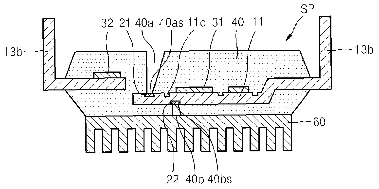
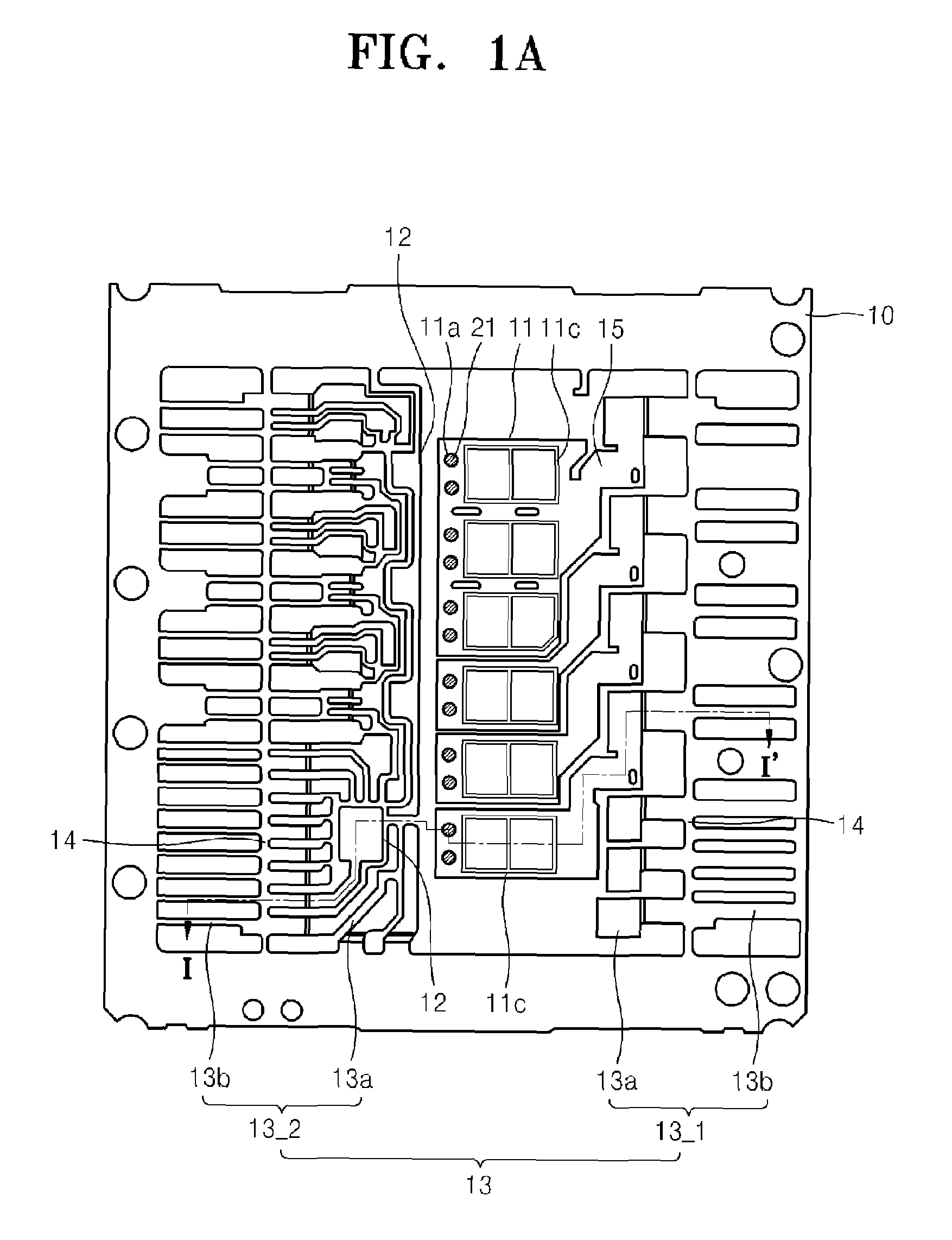
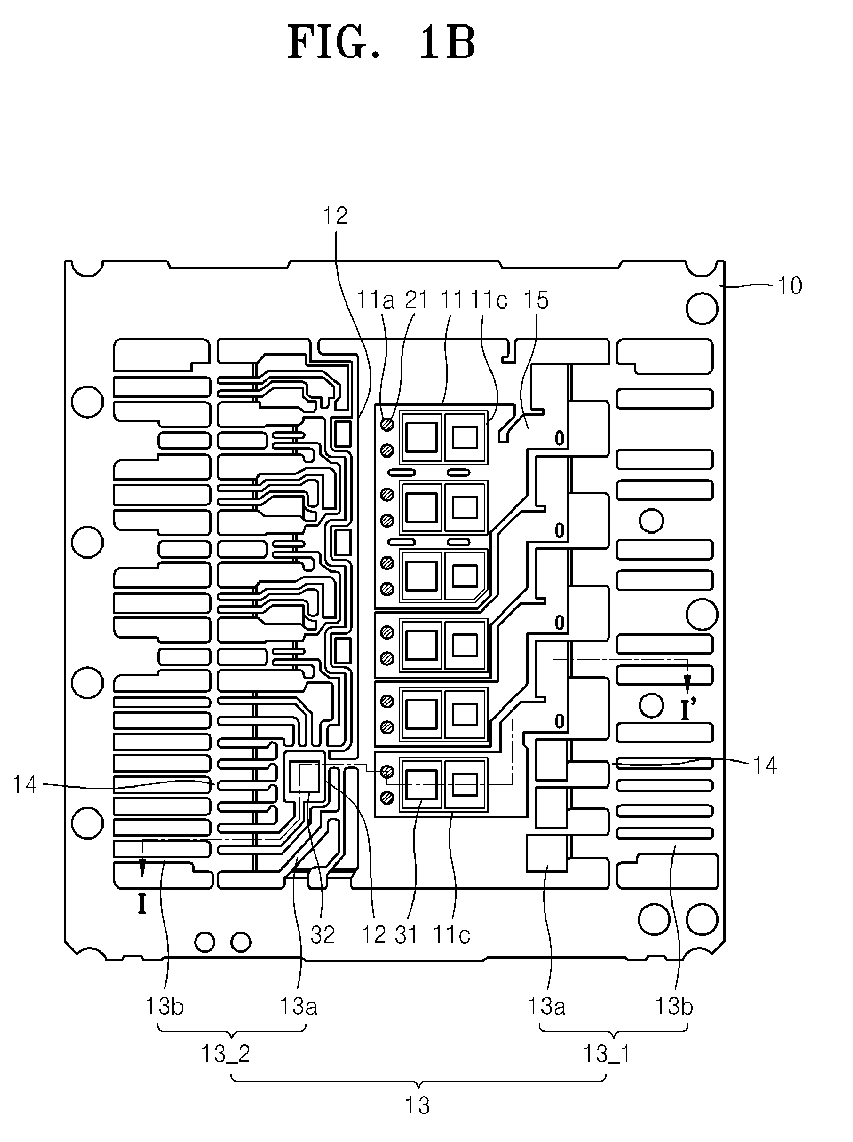
[0019]The present invention will now be described more fully hereinafter with reference to the accompanying drawings, in which exemplary embodiments of the invention are shown. This invention may, however, be embodied in different forms and should not be construed as limited to the embodiments set forth herein. Rather, these embodiments are provided so that this disclosure is thorough and complete and fully conveys the scope of the invention to one skilled in the art. It will also be understood that when a layer is referred to as being “on” another layer or substrate, it can be directly on the other layer, or substrate or intervening layers may also be present. In the drawings, the thicknesses of layers and regions are exaggerated for clarity. The same reference numerals are used to denote the same elements throughout the specification. The term “and / or” used herein includes any and all combinations of one or more of the associated listed items.

[0020]Like reference numerals refer to...


PUM


Abstract

Provided are semiconductor packages and methods of fabricating the same. An exemplary semiconductor package includes a die pad including a dimple filled with an insulating material in an upper surface or a lower surface thereof. A semiconductor chip is mounted on the upper surface of the first die pad. A package body encapsulates the first die pad and the first semiconductor chip and includes a pinhole. A bottom surface of the pinhole terminates at the insulating material.

Description

CROSS-REFERENCES TO RELATED APPLICATIONS[0001]This application claims the benefit of Korean Patent Application No. 10-2007-0112312, filed on Nov. 5, 2007, in the Korean Intellectual Property Office, the disclosure of which is incorporated herein in its entirety by reference.BACKGROUND OF THE INVENTION[0002]1. Field of the Invention[0003]The present invention relates to semiconductor packages and methods of fabricating the same, and more particularly, to semiconductor packages, each of which includes a semiconductor chip and a die pad encapsulated by a package body, and methods of fabricating such semiconductor packages.[0004]2. Description of the Related Art[0005]Fabrication of a semiconductor package typically involves mounting a semiconductor chip on an upper surface of a die pad included in a lead frame and forming a package body to encapsulate the semiconductor chip and the die pad.[0006]When the semiconductor chip is a highly integrated chip or a power circuit chip for controll...

Claims


Application Information

Patent Timeline
Patent Type & Authority Patents(United States)
IPC IPC(8): H01L23/28
CPCH01L21/565H01L23/3142H01L23/49503H01L23/49531H01L23/49575H01L24/82H01L23/3107H01L2924/00014H01L2924/13055H01L2924/13091H01L2924/1815H01L2224/45124H01L2924/1305H01L2224/45144H01L2924/1306H01L2924/00H01L2224/48H01L2924/181H01L23/28H01L23/02H01L23/00
Inventor SON, JOON-SEOJEON, O-SOEB
Owner SEMICON COMPONENTS IND LLC
Why Eureka
Try Eureka