Flash memory device and method of fabricating the same

a flash memory and memory cell technology, applied in the field of flash memory devices, can solve the problems of affecting the reliability of the memory cell, and more likely to occur step-coverage failure of the isolation structure,

Active Publication Date: 2010-05-18
SK HYNIX INC
View PDF9 Cites 1 Cited by
  • Summary
  • Abstract
  • Description
  • Claims
  • Application Information

AI Technical Summary

Benefits of technology

[0032]As described above, the embodiments of the present invention has one or more of the following advantages. First, the gate oxide breakdown is reduced since an isolation structure is formed at a boundary region if a gate line is to be provided over that boundary region. Second, an active region is formed at a boundary region if a gate line is not to be provided over that boundary region to minimize the likelihood of damage to the semiconductor substrate during a subsequent thermal process. Third, the well pickup region is formed within the active region to reduce the device size.

Problems solved by technology

The step-coverage failure of the isolation structure is more likely to occur as the isolation trench is provided with a smaller pitch.
The step-coverage failure in the memory cell region can be quite serious.
The step-coverage failure may generate a void in the isolation structure of the memory cell that can affect the reliability of the memory cell.
This would result in device failure.

Method used


Image

  • Flash memory device and method of fabricating the same
  • Flash memory device and method of fabricating the same
  • Flash memory device and method of fabricating the same

Examples


Embodiment Construction

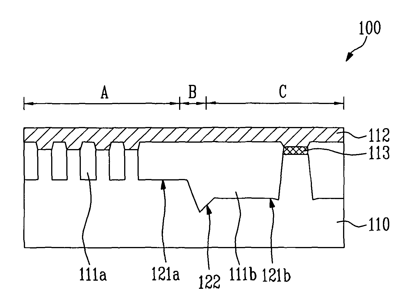
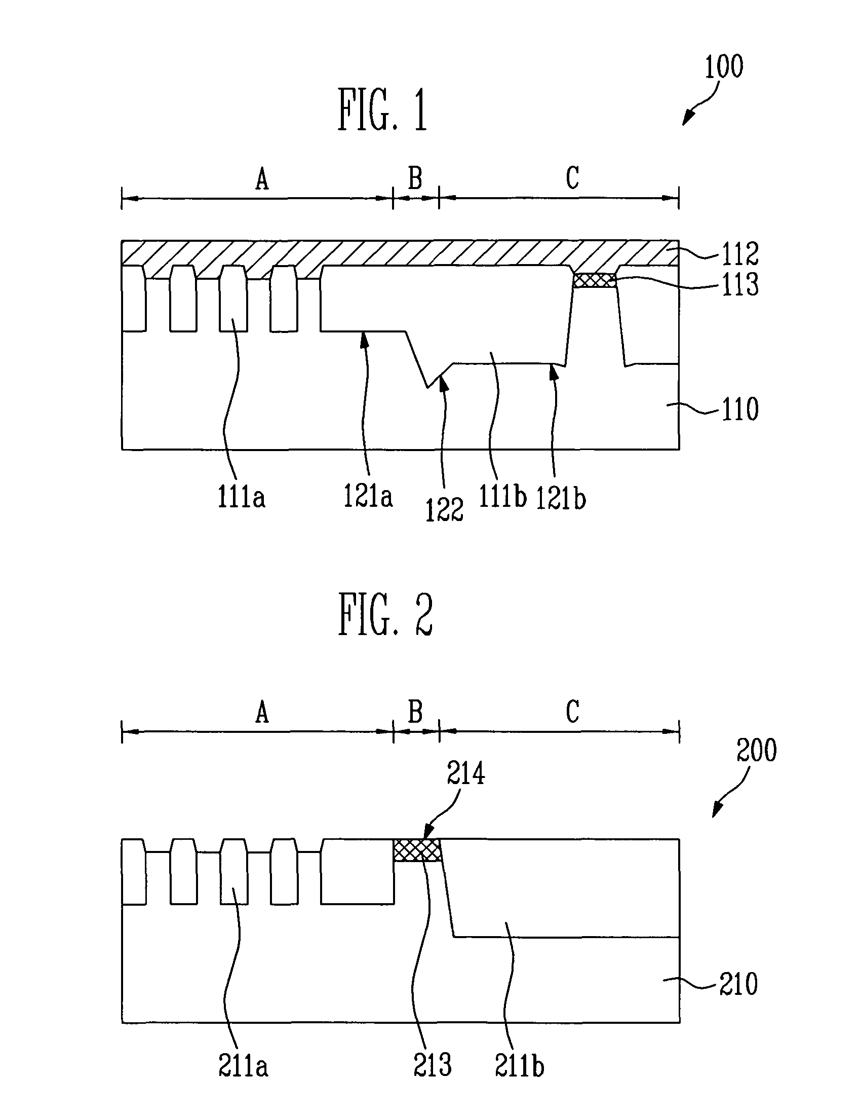
[0017]The present invention relates to forming a boundary region between a cell region and a peripheral region in a memory device, e.g., a NAND flash memory device. The type of the boundary region formed depends on whether or not a gate line is provided over the boundary region according to embodiments of the present invention. For example, a field oxide structure (FOX) is formed if a gate line is provided over the boundary region and an active region is formed when a gate line is not provided over the boundary region.

[0018]FIG. 1 illustrates a cross-sectional view of a flash memory device 100 having an isolation structure 111b at a boundary region B between a cell region A and a peripheral region C according to one embodiment of the present invention. The flash memory device 100 has a semiconductor substrate 110, a plurality of isolation structures 111a in the cell region A, an isolation structure 111b at the boundary region B, a gate line 112, and a well pickup region 113 in the p...


PUM


Abstract

A semiconductor device includes a semiconductor substrate having a cell region and a peripheral region. A cell array is defined within the cell region, the cell array having first, second, third, and fourth sides. A first decoder is defined within the peripheral region and provided adjacent to the first side of the cell array. A first isolation structure is formed at a first boundary region provided between the first side of the cell array and the peripheral region. A first dummy active region is formed at a second boundary region that is provided between the second side of the cell array and the peripheral region. The first isolation structure has a first portion that has a first depth and a second portion that has a second depth.

Description

CROSS-REFERENCES TO RELATED APPLICATIONS[0001]The present application claims priority to Korean patent application number 2005-72323, filed on Aug. 8, 2005, which is incorporated by reference.BACKGROUND OF THE INVENTION[0002]The present invention relates to a memory device and method of fabricating the same, and more particularly, to forming a boundary region between cell and peripheral regions in the memory device.[0003]In the memory device, e.g., the NAND flash, the pitch of the isolation trench is becoming smaller and smaller as the technology advances. The isolation trench is gap-filled with an oxide film to form field oxide structure (FOX) or isolation structure. Such an oxide film is typically formed using High Density Plasma (HDP) method. The step-coverage failure of the isolation structure is more likely to occur as the isolation trench is provided with a smaller pitch.[0004]The step-coverage failure in the memory cell region can be quite serious. The step-coverage failure m...

Claims


Application Information

Patent Timeline
Patent Type & Authority Patents(United States)
IPC IPC(8): H01L29/76
CPCH01L27/11531H01L27/11526H01L27/105G11C16/0408H10B41/40H10B41/42H10B99/00
Inventor PARK, SUNG KEE
Owner SK HYNIX INC
Why Eureka
Try Eureka