Semiconductor package and manufacturing method thereof

a technology of semiconductors and packaging, applied in the field of packaging, can solve the problems of difficult control of signals and limited stacking number of packages, and achieve the effect of improving stacking package performan

Active Publication Date: 2010-05-18
ADVANCED SEMICON ENG INC
View PDF5 Cites 33 Cited by
  • Summary
  • Abstract
  • Description
  • Claims
  • Application Information

AI Technical Summary

Benefits of technology

[0009]Accordingly, the present invention is directed to a semiconductor package and a manufacturing method thereof, capable of increasing the number of I / O ports and improving a stacking package performance.
[0012]Accordingly, in the semiconductor package and the manufacturing method thereof according to the present invention, the second conductive part of the lead frame is electrically connected to the third conductive part of the lead frame, so as to serve as the I / O port of the externally connected electronic device stacked on the semiconductor package. The first conductive part is not electrically connected to the second conductive part, so as to serve as the I / O port of the chip. As compared with the conventional art, the chip of the semiconductor package of the present invention may transmit signals through the first conductive part, and the externally connected electronic device may transmit signals through the second conductive part and the third conductive part, such that the semiconductor package may provide more I / O ports on the first surface to support more signal transmission, thereby improving the stacking package performance.

Problems solved by technology

However, for signal transmission, the chips 111, 121, 131, and 141 share the lead frame 112 as an input / output (I / O) port, such that it is difficult to control the signal.
Because of the limit of the number of the I / O ports, the semiconductor package device 1 is not applicable to package the chip with complicated wires, and the stacking number of the package may also be limited.

Method used


Image

  • Semiconductor package and manufacturing method thereof
  • Semiconductor package and manufacturing method thereof
  • Semiconductor package and manufacturing method thereof

Examples


Embodiment Construction

[0021]In the following, referring to relative drawings, a semiconductor package and a manufacturing method thereof according to an embodiment of the present invention are described, in which the same elements are marked by the same reference numerals.

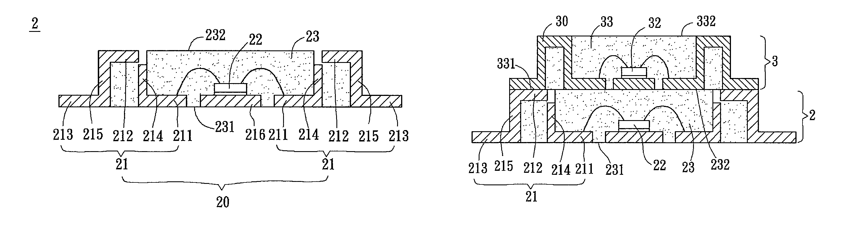
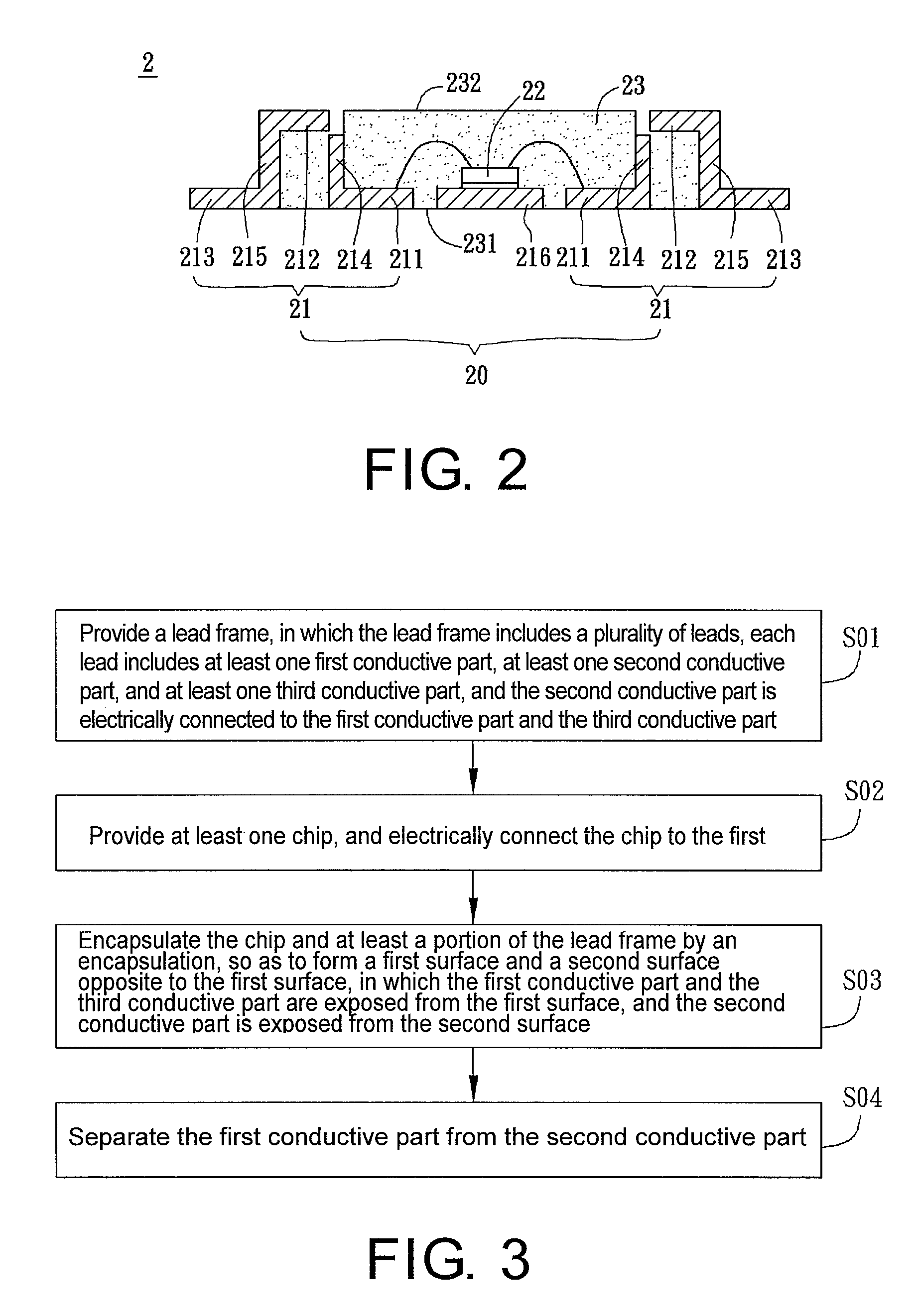
[0022]Referring to FIG. 2, a semiconductor package 2 according to an embodiment of the present invention includes a lead frame 20, at least one chip 22, and an encapsulation 23. In this embodiment, the semiconductor package 2 is, for example, but not limited to, a quad flat package (QFP).

[0023]The lead frame 20 has a plurality of leads 21, in which each lead 21 includes at least one first conductive part 211 at least one second conductive part 212, and at least one third conductive part 213. The first conductive part 211 is not electrically connected to the second conductive part 212, and the second conductive part 212 is electrically connected to the third conductive part 213. An uplifting portion 214 is disposed between the first cond...


PUM


Abstract

A semiconductor package includes a lead frame, at least one chip, and an encapsulation. The lead frame has a plurality of leads, and each of the leads includes at least one first conductive part, at least one second conductive part, and at least one third conductive part. The first conductive part is not electrically connected to the second conductive part, and the second conductive part is electrically connected to the third conductive part. The chip is electrically connected to the first conductive part. The encapsulation encapsulates the chip and at least a portion of the lead frame, and forms a first surface and a second surface opposite to the first surface. The first conductive part and the third conductive part are exposed from the first surface, and the second conductive part is exposed from the second surface.

Description

CROSS-REFERENCE TO RELATED APPLICATION[0001]This application claims the priority benefit of Taiwan application serial no. 96135077, filed on Sep. 20, 2007. The entirety of the above-mentioned patent application is hereby incorporated by reference herein and made a part of specification.BACKGROUND OF THE INVENTION[0002]1. Field of the Invention[0003]The present invention generally relates to a package and a manufacturing method thereof, in particular, to a semiconductor package having a lead frame and a manufacturing method thereof.[0004]2. Description of Related Art[0005]In the semiconductor technology development, the capacity and performance of semiconductor package devices are improved to meet the demands of users along with the miniaturization and high-efficiency oriented development of electronic products. Therefore, multi-chip module becomes one of the researching focuses in recent years, in which a semiconductor package device is formed by stacking two or more chips, thereby ...

Claims


Application Information

Patent Timeline
Patent Type & Authority Patents(United States)
IPC IPC(8): H01L23/495H01L21/44H01L21/48H01L21/50
CPCH01L23/49551H01L23/49572H01L25/105H01L25/50H01L23/3107H01L2225/1058H01L2225/1041H01L2225/1029H01L2224/85H01L2224/32245H01L24/16H01L24/48H01L24/81H01L24/85H01L2224/48091H01L2224/48247H01L2224/73265H01L2224/81801H01L2224/16245H01L2924/00014H01L2924/00012H01L24/73H01L2924/181H01L2224/45099H01L2224/45015H01L2924/207
Inventor WU, CHIA-FULEE, CHENG-YIN
Owner ADVANCED SEMICON ENG INC
Why Eureka
Try Eureka