
Active device array substrate

a technology of active devices and array substrates, applied in the direction of individual semiconductor device testing, semiconductor/solid-state device testing/measurement, instruments, etc., can solve the problem of active device array substrates

Inactive Publication Date: 2010-05-25
E INK HLDG INC
View PDF5 Cites 5 Cited by
  • Summary
  • Abstract
  • Description
  • Claims
  • Application Information

AI Technical Summary

Benefits of technology

This solution significantly reduces the risk of electrostatic damage to the circuits, enhancing the stability and reliability of the active device array substrate by preventing charge transfer from testing pads to the display area.

Problems solved by technology

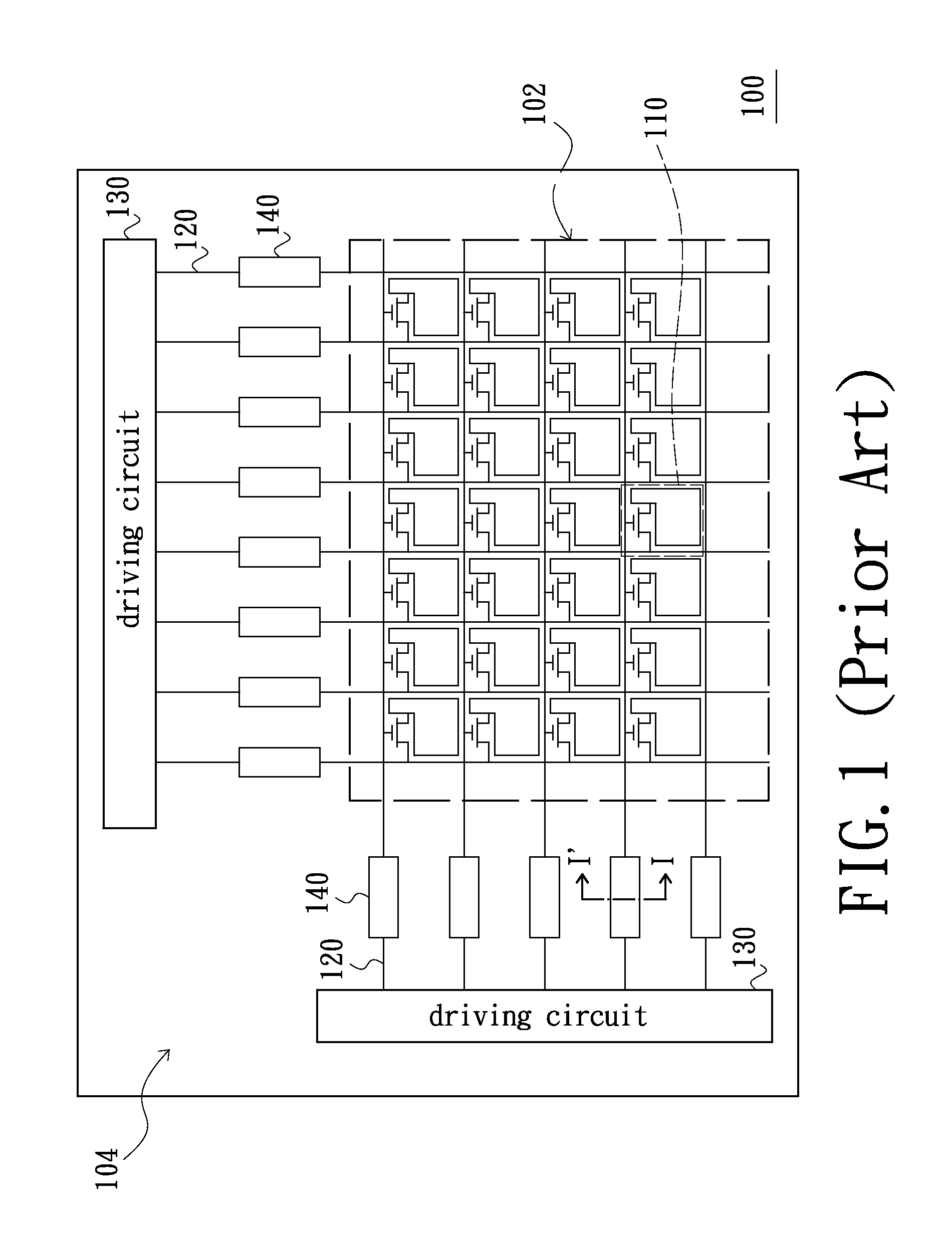
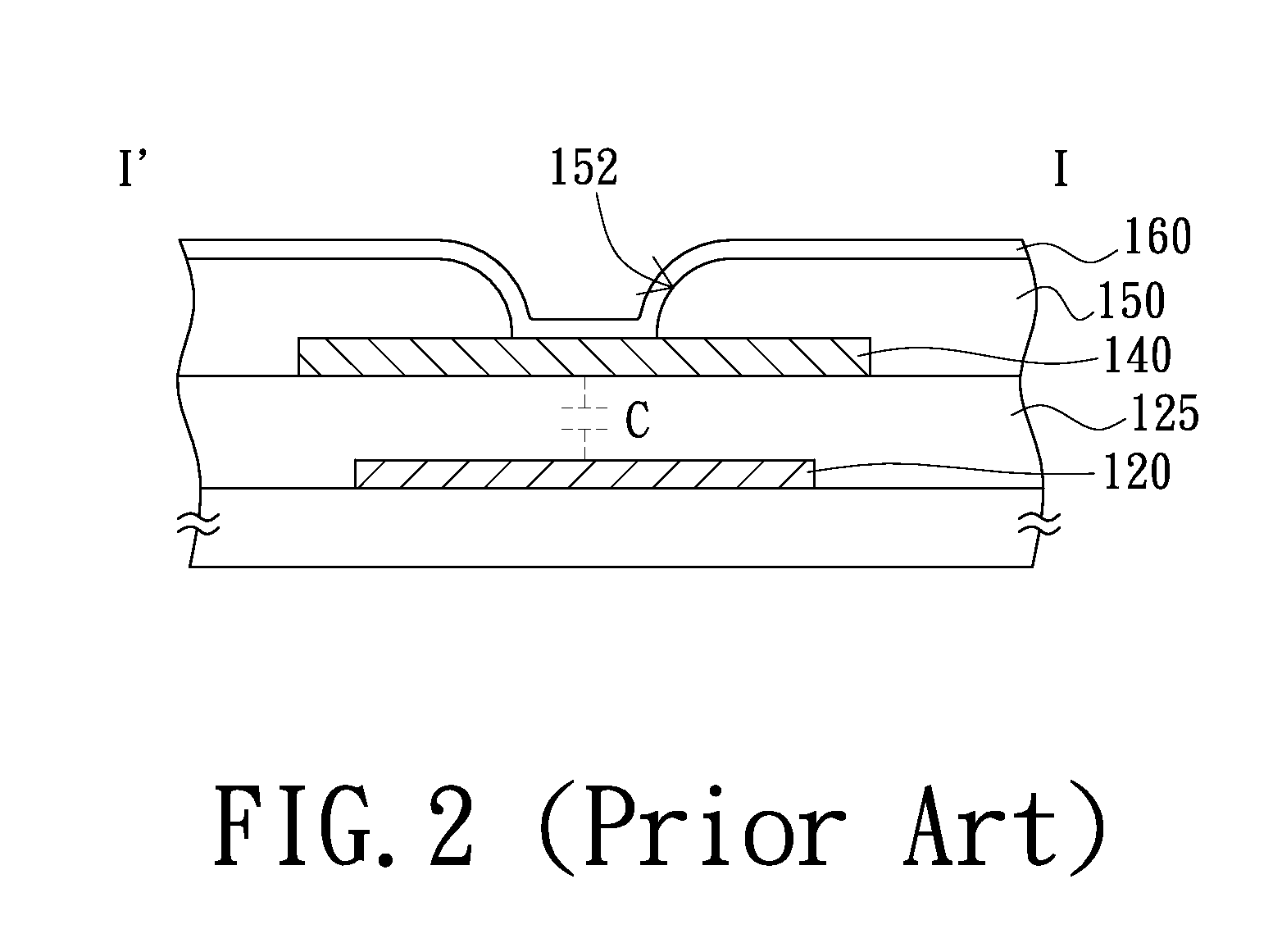
As a result, the circuits in the display area 102 would suffer from electrostatic damage so that the active device array substrate 100 is destroyed.

Method used


Image

  • Active device array substrate
  • Active device array substrate
  • Active device array substrate

Examples


Embodiment Construction

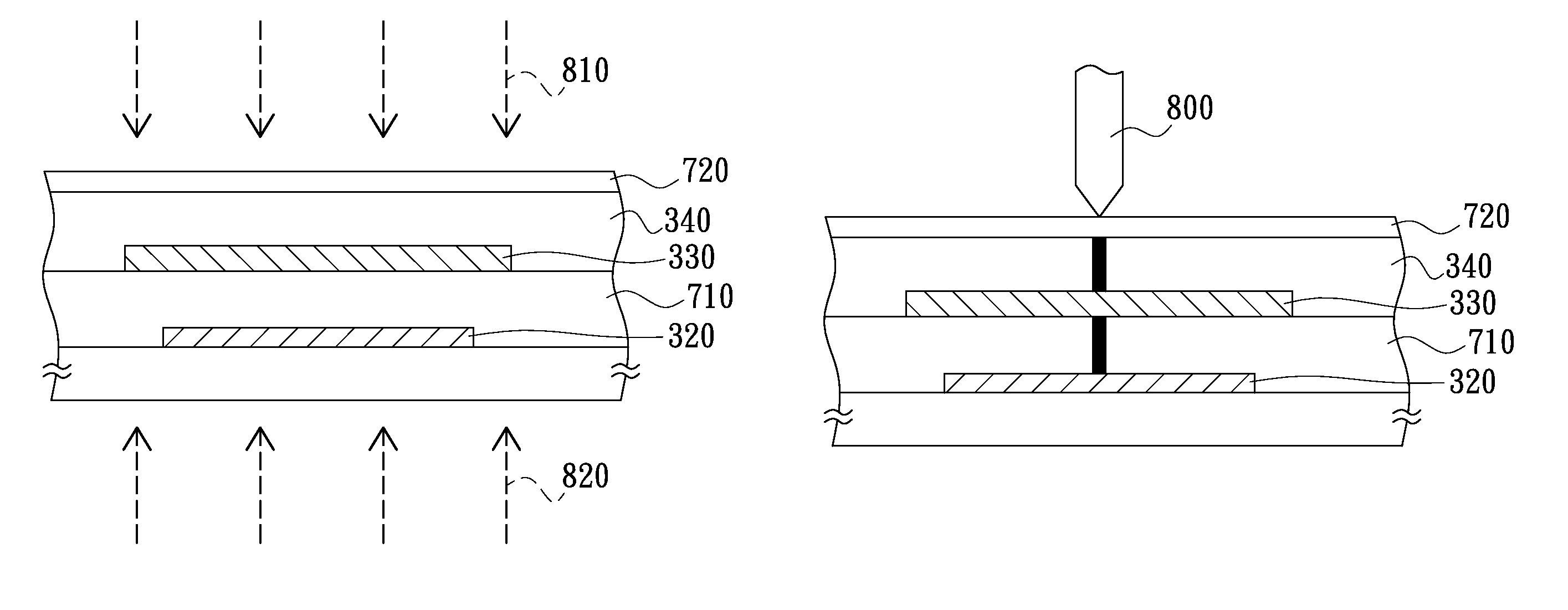
[0032]FIG. 3 is a schematic view of an active device array substrate in accordance with an embodiment of the present invention. FIG. 4 is a sectional view of the active device array substrate at the location where a testing pad is disposed. Referring to FIGS. 3 and 4, the active device array substrate 300 having a display area 302 and a peripheral circuit area 304 comprises a plurality of pixel units 310, a plurality of signal lines 320, a plurality of testing pads 330 and a first dielectric layer 340. The pixel units 310 are arranged in the display area 302 in an array.

[0033]More specifically, each of the pixel unit 310 for example is consisted of a scan line 312, a data line 314, an active device 316 and a pixel electrode 318. The scan line 312 and the data line 314 are substantially perpendicular to each other. The active device 312 and the pixel electrode 318 are disposed in a region surrounded by the scan line 312 and the data line 314. The active device 316 is electrically con...


PUM


Abstract

An active device array substrate has a display area and a peripheral circuit area and further includes a plurality of pixel units, a plurality of signal lines, a plurality of testing pads and a first dielectric layer. The pixel units are arranged in the display area in an array. The signal lines and the testing pads are arranged in the peripheral circuit area. The first dielectric layer covers the testing pads. A testing method of the active device array substrate is that firstly removing a part of the first dielectric layer to expose a testing pad(s) desired to electrically contact with a testing tool. In other words, before the testing, the testing pads are electrically insulated from the exterior to prevent the pixel units from the electrostatic charges damage and thus the circuit stability of the active device array substrate can be improved.

Description

BACKGROUND[0001]1. Technical Field[0002]The present invention generally relates to an active device array substrate and a testing method thereof and, particularly to, an active device array substrate which can prevent circuits thereof from being damaged by electrostatic charges through testing pads and a testing method of the active device array substrate.[0003]2. Description of the Related Art[0004]Since active flat display panels have the advantages of small size, light weight and fast response, the active flat display panels are widely applied on various electronic products. An active flat display panel generally is consisted of an active device array substrate, a display layer and a light-transmissive substrate. The display layer is sandwiched between the active device array substrate and the light-transmissive substrate and can be, for example a liquid crystal layer of a liquid crystal display (LCD) panel or an electrophoretic layer of an electrophoretic display (EPD) panel and...

Claims


Application Information

Patent Timeline
Patent Type & Authority Patents(United States)
IPC IPC(8): G01R31/02G01R31/26
CPCG02F1/13458G02F1/1362G09G3/006G02F2001/136254G02F1/136254
Inventor CHANG, HENG-HAOLIU, CHUAN-FENG
Owner E INK HLDG INC
Learn More