

Active device array substrate
a technology of active devices and array substrates, applied in the direction of static indicating devices, semiconductor/solid-state device testing/measurement, instruments, etc., can solve the problems of active device array substrates
- Summary
- Abstract
- Description
- Claims
- Application Information
AI Technical Summary
Benefits of technology
Problems solved by technology
Method used
Image

Examples
Embodiment Construction
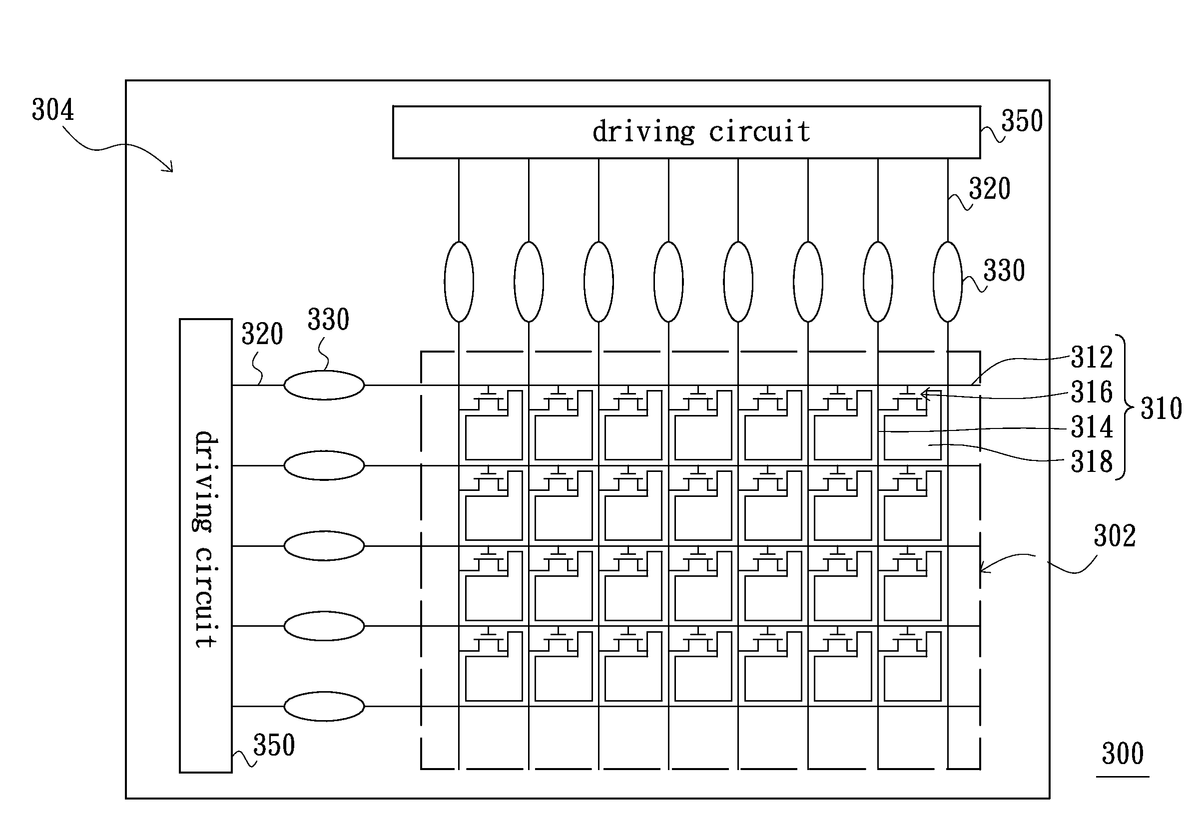
[0032]FIG. 3 is a schematic view of an active device array substrate in accordance with an embodiment of the present invention. FIG. 4 is a sectional view of the active device array substrate at the location where a testing pad is disposed. Referring to FIGS. 3 and 4, the active device array substrate 300 having a display area 302 and a peripheral circuit area 304 comprises a plurality of pixel units 310, a plurality of signal lines 320, a plurality of testing pads 330 and a first dielectric layer 340. The pixel units 310 are arranged in the display area 302 in an array.
[0033]More specifically, each of the pixel unit 310 for example is consisted of a scan line 312, a data line 314, an active device 316 and a pixel electrode 318. The scan line 312 and the data line 314 are substantially perpendicular to each other. The active device 312 and the pixel electrode 318 are disposed in a region surrounded by the scan line 312 and the data line 314. The active device 316 is electrically con...
PUM
 Abstract
Description
Claims
Application Information