Controlled composition using plasma-enhanced atomic layer deposition

a technology of atomic layer and controlled composition, which is applied in the direction of chemical vapor deposition coating, coating, semiconductor devices, etc., can solve the problems of inability to avoid local concentration variations over the substrate, insufficient polysilicon work functions, and inability to predict and control the work functions of metal gate materials after doping, etc., to achieve the effect of easily and accurately adjusting to a desired valu

Active Publication Date: 2010-06-01
ASM IP HLDG BV
View PDF17 Cites 395 Cited by
  • Summary
  • Abstract
  • Description
  • Claims
  • Application Information

AI Technical Summary

Benefits of technology

[0016]It is an object of the present invention to provide an improved method of depositing an integrated circuit, in which method the composition, hence the work function of the gate electrode can be easily and accurately adjusted to a desired value.

Problems solved by technology

However, in current technology, polysilicon is no longer adequate because of its relatively low conductivity and because of depletion effects.
However, work functions of metal gate materials after doping are not easily predictable and controllable.
However, a method avoiding local concentration variations over the substrate is not disclosed.
However, the electrodes were formed by physical vapor deposition (PVD), resulting in sputtering damage on the gate stack dielectric layer and, furthermore, causing non-uniformities in electrical and physical properties of ultra-thin films over the substrate.
A problem associated with the known methods of tuning the work function of a gate stack is that adequate control of film composition, uniformities and profiles, or thickness cannot be achieved.
Further, subjecting the gate electrode material to an oxidizing ambient subjects the gate dielectric material also to the oxidizing ambient, which might detrimentally affect the dielectric material and oxidize the underlying substrate material.

Method used


Image

  • Controlled composition using plasma-enhanced atomic layer deposition
  • Controlled composition using plasma-enhanced atomic layer deposition
  • Controlled composition using plasma-enhanced atomic layer deposition

Examples


Embodiment Construction

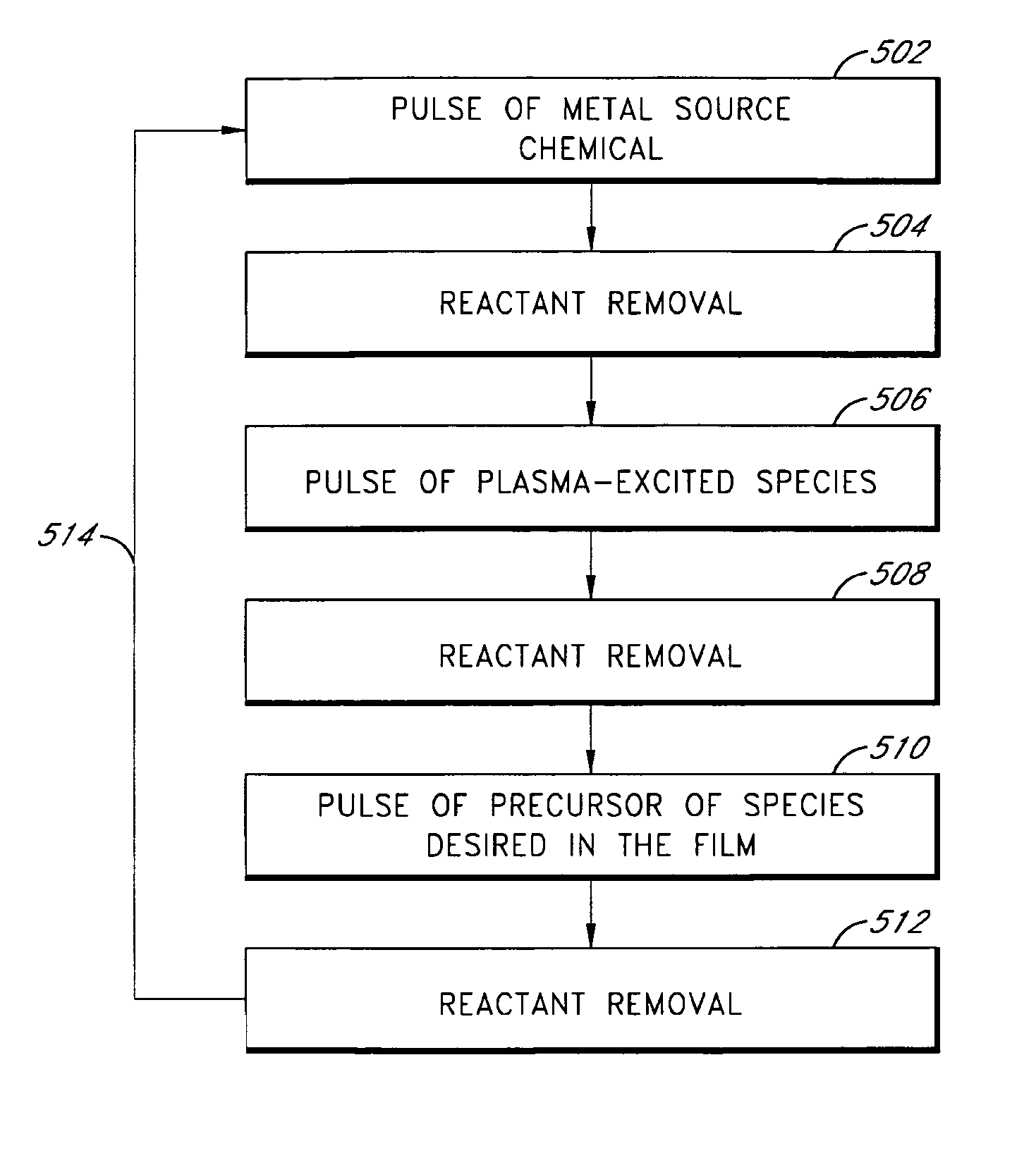
[0033]The disclosed methods will be described in detail by way of preferred embodiments with reference to accompanying drawings. Although described in the context of certain preferred embodiments, the skilled artisan will appreciate, in view of the disclosure herein, that the materials, methods and structures described herein will have a variety of other applications.

[0034]According to preferred embodiments of the invention, metallic-compound films or thin films comprising a metal or a plurality of metals and at least one other species desired in the film (e.g., carbon, nitrogen, oxygen, or silicon) are formed by a plasma-enhanced atomic layer deposition (PEALD) process. The stoichiometry, hence the composition of the films is selected based upon plasma parameters during film deposition. By selecting plasma parameters during film deposition, non-stoichiometric metallic-compound films, preferably metal-rich metallic-compound films, may be formed with compositions as desired. Such fil...


PUM

PropertyMeasurementUnit
electrical thicknessaaaaaaaaaa
work functionaaaaaaaaaa

Abstract

Metallic-compound films are formed by plasma-enhanced atomic layer deposition (PEALD). According to preferred methods, film or thin film composition is controlled by selecting plasma parameters to tune the oxidation state of a metal (or plurality of metals) in the film. In some embodiments, plasma parameters are selected to achieve metal-rich metallic-compound films. The metallic-compound films can be components of gate stacks, such as gate electrodes. Plasma parameters can be selected to achieve a gate stack with a predetermined work function.

Description

REFERENCE TO RELATED APPLICATIONS[0001]The present application is related to U.S. patent application Ser. No. 10 / 430,703 to Huotari et al., filed May 5, 2003, now U.S. Pat. No. 7,045,406, the disclosure of which is incorporated entirely by reference herein.FIELD OF THE INVENTION[0002]The present invention relates generally to the deposition of metallic-compound films or thin films and more particularly to atomic layer deposition (ALD) for the field of semiconductor manufacturing.BACKGROUND OF THE INVENTION[0003]Semiconductor devices are continuously improved to enhance device performance. For example, both smaller device size and higher speed of operation are highly desirable performance targets. Transistors have also been continuously reduced in size to lower the power consumption and to increase the clocking frequency. By constructing smaller gate structures for complementary metal oxide silicon (CMOS) transistors, it becomes possible to pack more transistors on the same surface a...

Claims


Application Information

Patent Timeline
Patent Type & Authority Patents(United States)
IPC IPC(8): H01L21/3065
CPCC23C16/45525C23C16/4554H01L21/28088H01L29/4966C23C16/50H01L29/517
Inventor ELERS, KAI-ERIK
Owner ASM IP HLDG BV
Why Eureka
Try Eureka