Multi-domain liquid crystal with axisymmetric alignment and electrode having asymmetrical cuts at the edge

a liquid crystal and electrode technology, applied in the field of multi-domain liquid crystals with axisymmetric alignment and electrodes with asymmetric cuts at the edges, can solve the problems of difficult to generate inclined electric fields over the entire region of each pixel, occurrence of afterimage phenomena, and complicating the fabrication process, so as to reduce the effective aperture ratio, improve the uniformity of display, and improve the effect of uniformity

Inactive Publication Date: 2010-06-01
SHARP KK
View PDF26 Cites 32 Cited by
  • Summary
  • Abstract
  • Description
  • Claims
  • Application Information

AI Technical Summary

Benefits of technology

[0032]In the liquid crystal display device of the present invention, the directions in which liquid crystal molecules tilt during voltage application (during generation of an electric field) are defined with the slope face effect of the wall structure formed on the surface of the first substrate facing the liquid crystal layer in the shading region, so that an axisymmetrically aligned domain is formed. Also, a hole formed in the color filter layer of the second substrate opposed to the first substrate acts to fix the position of the center axis of the axisymmetric alignment at or near the hole, and this stabilizes the alignment of the axisymmetrically aligned domain.
[0033]Since the wall structure formed on the first substrate is located in the shading region, an axisymmetrically aligned domain can be formed without causing reduction in effective aperture ratio or contrast ratio.
[0036]The reduction in effective aperture ratio due to the existence of the opening can be minimized by placing the first opening formed in the first electrode and the hole in the color filter layer of the second substrate so as to at least overlap each other via the liquid crystal layer. Since one center axis is fixed / stabilized with the joint action of the first opening and the hole in the color filter layer, the action of the opening and the hole can be exerted more effectively.
[0037]According to the present invention, the position of the center axis of each axisymmetrically aligned liquid crystal domain is fixed / stabilized. As a result of the fixation of the center axes of the axisymmetrically aligned liquid crystal domains over the entire liquid crystal display panel, the uniformity of the display improves. Accordingly, the roughness of display recognized when grayscale display is viewed in a slanting direction is reduced, and also the response time in grayscale display can be shortened. In addition, as a result of the stabilization of the axisymmetric alignment, the time required to resume normal alignment from an alignment distortion occurring when the liquid crystal display panel is pressed (an afterimage due to pressing) can be shortened.
[0038]By forming an opening in the second electrode at the position corresponding to the hole in the color filter layer, the alignment regulating force with an inclined electric field can be increased to fix the center axis further stably. However, since no patterning is involved in formation of the counter electrode as the second electrode that covers roughly the entire surface of the liquid crystal panel, an additional step is required to form the second opening in the second electrode. On the contrary, pattering is involved in formation of the color filter layer to provide individual color layers. Holes can therefore be formed during this patterning with no additional step required. In other words, according to the present invention, the center axes of axisymmetric alignment can be fixed / stabilized without the necessity of forming second openings in the second electrode, that is, without the necessity of increasing the number of fabrication steps.
[0039]When the present invention is applied to a transflective LCD device, a transparent dielectric layer may be placed on the second substrate for control of the thickness of the liquid crystal layer. With this construction, an invalid region that does not contribute to display during transmission display can be reduced compared with the conventional transflective LCD device in which the transmission region and the reflection region are differentiated from each other by forming a step on the first substrate, and thus the brightness in transmission display can be improved. The diffuse reflection plate for improving the brightness in the reflection region may be provided on the first substrate in the reflection region. Otherwise, a light scattering layer (light diffuse layer) may be formed on the transparent dielectric layer on the second substrate. This can eliminate the necessity of forming projections and depressions on the surface of the reflection electrode.

Problems solved by technology

However, in the device described in Literature 1, it is difficult to generate an inclined electric field over the entire region of each pixel.
Therefore, each pixel has a region in which liquid crystal molecules delay in response to a voltage, and this causes a problem of occurrence of an afterimage phenomenon.
According to examinations conducted by the inventors of the present invention, however, to obtain sufficient alignment regulating force, it is necessary to form an alignment control structure made of projections regularly placed inside each pixel, and this complicates the fabrication process.
This technology therefore has the same problems as those described above.

Method used


Image

  • Multi-domain liquid crystal with axisymmetric alignment and electrode having asymmetrical cuts at the edge
  • Multi-domain liquid crystal with axisymmetric alignment and electrode having asymmetrical cuts at the edge
  • Multi-domain liquid crystal with axisymmetric alignment and electrode having asymmetrical cuts at the edge

Examples


Embodiment Construction

[0049]Hereinafter, LCD devices of an embodiment of the present invention will be described concretely with reference to the relevant drawings.

(Transmissive LCD Device)

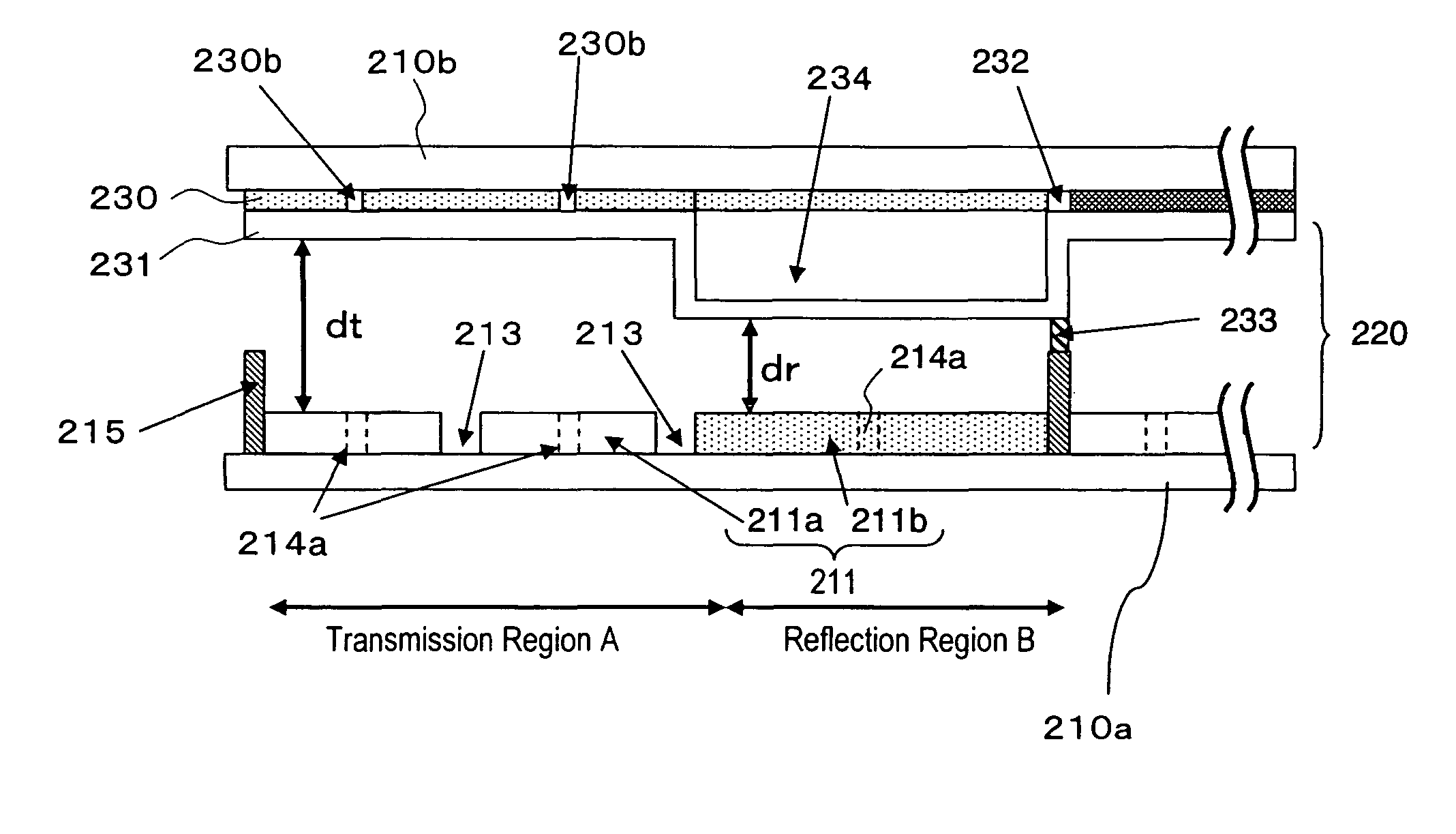
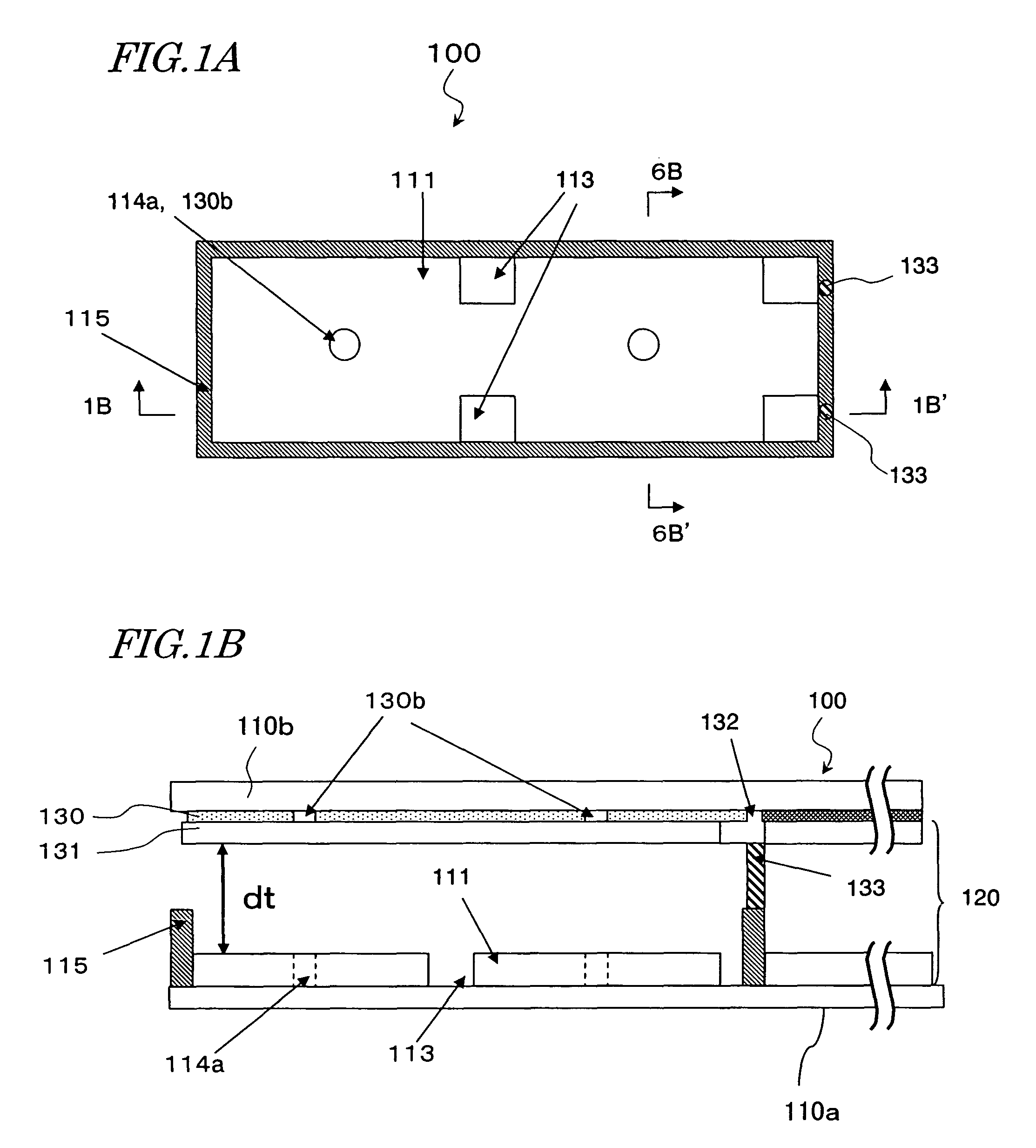
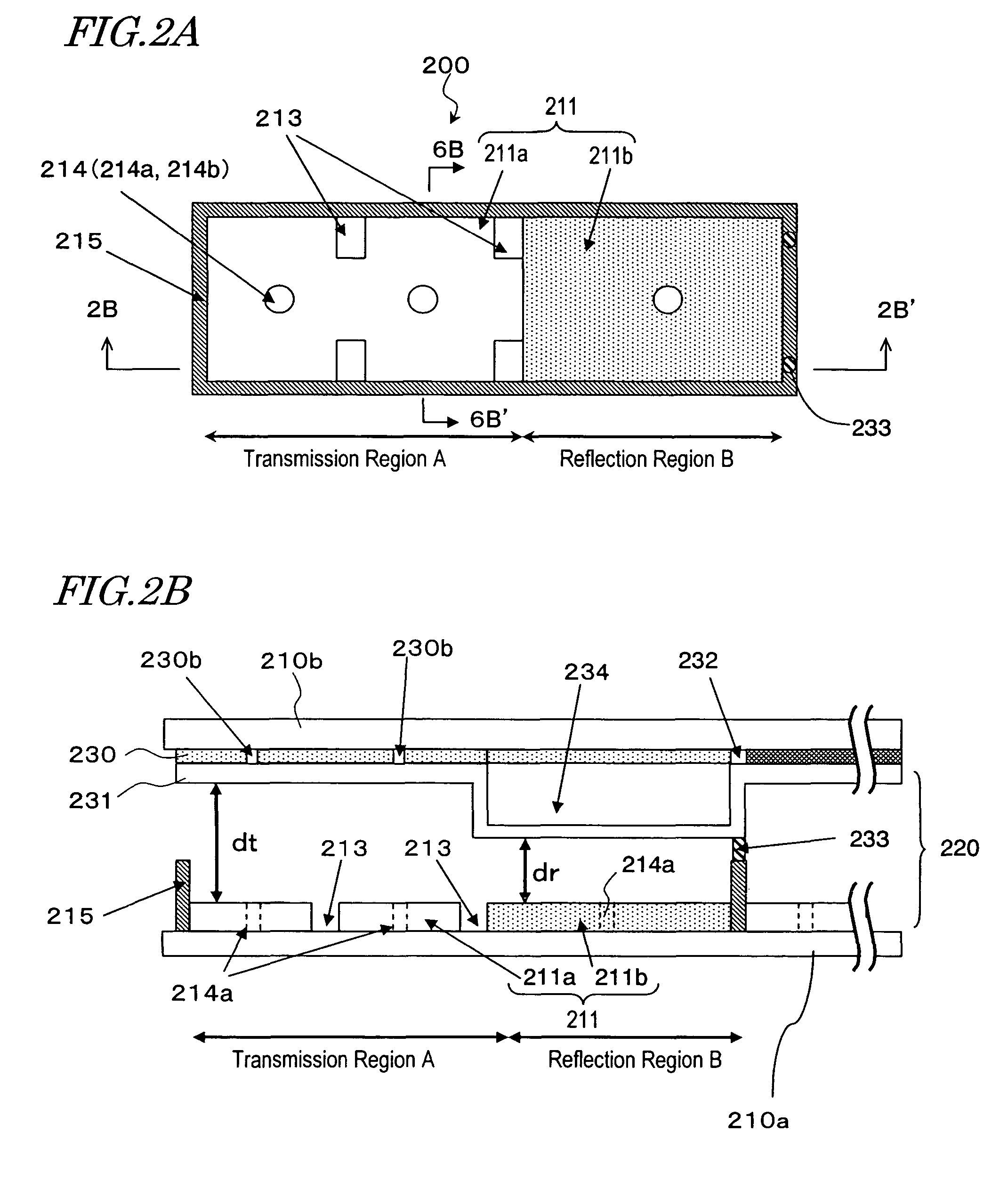
[0050]A transmissive LCD device 100 of the embodiment of the present invention will be described with reference to FIGS. 1A and 1B. FIGS. 1A and 1B diagrammatically show one pixel of the transmissive LCD device 100, in which FIG. 1A is a plan view and FIG. 1B is a cross-sectional view taken along line 1B-1B′ in FIG. 1A.

[0051]Hereinafter, described will be the case that one pixel is divided into two parts (N=2). The number of parts into which one pixel is divided (=N) can also be three or more depending on the pixel pitch. In any case, the number of openings (=n) each to be positioned roughly in the center of a divided region on a second substrate is preferably the same as the number of divided parts (=N). The effective aperture ratio tends to decrease with increase of the number of divided parts (=N). Therefore, for an...


PUM

PropertyMeasurementUnit
transmittanceaaaaaaaaaa
thicknessaaaaaaaaaa
reflectanceaaaaaaaaaa

Abstract

The liquid crystal display device includes a first substrate, a second substrate opposed to the first substrate, and a vertically aligned liquid crystal layer interposed between the first and second substrates, and has a plurality of pixels each including a first electrode formed on the first substrate, a second electrode formed on the second substrate, and the liquid crystal layer interposed between the first and second electrodes. The first substrate has a shading region in gaps between the plurality of pixels, and a wall structure is placed regularly on the surface of the first substrate facing the liquid crystal layer in the shading region. A color filter layer of the second substrate has at least one hole formed at a predetermined position in each pixel. At least one liquid crystal domain having axisymmetric alignment is formed in the liquid crystal layer when at least a predetermined voltage is applied across the liquid crystal layer, and the center axis of the axisymmetrically aligned liquid crystal domain is formed in or near the hole in the color filter layer.

Description

[0001]This application a U.S. patent application and claims priority to JP 2004-179889, filed 17 Jun. 2004, the entire content of which is hereby incorporated by reference.BACKGROUND OF THE INVENTION[0002]1. Field of the Invention[0003]The present invention relates to a liquid crystal display device and a fabrication method for the same, and more particularly, to a liquid crystal display device suitably used for portable information terminals (for example, PDAs), mobile phones, car-mounted liquid crystal displays, digital cameras, PCs, amusement equipment, TVs and the like.[0004]2. Description of the Related Art[0005]The information infrastructure is advancing day to day, and equipment such as mobile phones, PDAs, digital cameras, video cameras and car navigators has penetrated deeply into people's lives. Liquid crystal display (LCD) devices have been adopted in most of such equipment. With increase of the information amount handled with the main bodies of the equipment, LCD devices...

Claims


Application Information

Patent Timeline
Patent Type & Authority Patents(United States)
IPC IPC(8): G02F1/1335G02F1/1337G02F1/1339G02F1/1333G02F1/1368G02F1/139
CPCG02F1/133707G02F1/1393G02F1/133514G02F1/1368G02F1/13394
Inventor KUME, YASUHIROONISHI, NORIAKITAMAI, KAZUHIKOKOJIMA, HIROAKINAGAE, NOBUKAZU
Owner SHARP KK
Why Eureka
Try Eureka