Nonvolatile memory device

a memory device and non-volatile technology, applied in the direction of bulk negative resistance effect devices, instruments, basic electric elements, etc., can solve the problems of increasing the temperature of variable resistor elements, the speed of downsizing along a plane of flash memories is now close to its limit, etc., to reduce the program voltage applied to the selected memory, the effect of suppressing the diffusion of hea

Inactive Publication Date: 2011-01-04
XENOGENIC DEV LLC
View PDF7 Cites 34 Cited by
  • Summary
  • Abstract
  • Description
  • Claims
  • Application Information

AI Technical Summary

Benefits of technology

[0019]In an aspect of the present invention, the foregoing drawback in the conventional device is eliminated by providing a nonvolatile memory device arranged in which the variable resistor element in its selected memory cell is varied in the resistance while the resistance of the variable resistor element in an unselected memory cell located adjacent to the selected memory cell is inhibited from being varied by preventing heat generated in the variable resistor element from diffusing to the outside of the selected memory cell.
[0035]The nonvolatile memory device according to the present invention can suppress the diffusion of heat generated at the variable resistor element to the outside of the selected memory cell during the write action thus permitting no fault write action at any unselected memory cell located adjacent to the selected memory cell. Also, since the diffusion of heat is suppressed, the writing action at the selected memory cell can be increased in the efficiency. Accordingly, the program voltage applied to the selected memory can be decreased thus to minimize the current flowing through the selected memory cell during the program action of the selected memory cell.
[0036]FIG. 15A is a simulated profile of the temperature distribution between two adjacent memory cells in the nonvolatile memory device according to the present invention while FIG. 15B illustrates the same in the conventional device shown in FIG. 10. The nonvolatile memory device according to an inventive embodiment, unlike the conventional device, has the thermal diffusion barriers, which are 0.01 (W / cm·K) in thermal conductivity and 50 nm in thickness, disposed between the bit line and the memory cell and between the word line and the memory cell respectively. As apparent from the profile of FIG. 15, in the example nonvolatile memory device according to the present invention, even when the temperature of the variable resistor element in the selected memory cell is as high as about 920 K (647° C.), the variable resistor element in the adjacent unselected memory cell can remain at 300 K (27° C.) in temperature. In the conventional device, when the variable resistor element in the selected memory cell is at 920 K (647° C.) in temperature, the temperature of the variable resistor element in the adjacent unselected memory cell will be increased to 512 K (239° C.). It is therefore understood that the temperature in the adjacent unselected memory cell is effectively prevented from increasing by the presence of the thermal diffusion barriers which are lower in thermal conductivity than the bit lines and the word lines. The effect of suppressing the temperature rise in the adjacent memory cells can adjustably be controlled by modifying the thermal conductivity and the thickness of the thermal diffusion barriers.

Problems solved by technology

However, the downsizing along a plane of flash memories is now close to its limit.
This causes Joule heat in the selected memory cell hence increasing the temperature of the variable resistor element in the selected memory cell.

Method used


Image

  • Nonvolatile memory device
  • Nonvolatile memory device
  • Nonvolatile memory device

Examples


first embodiment

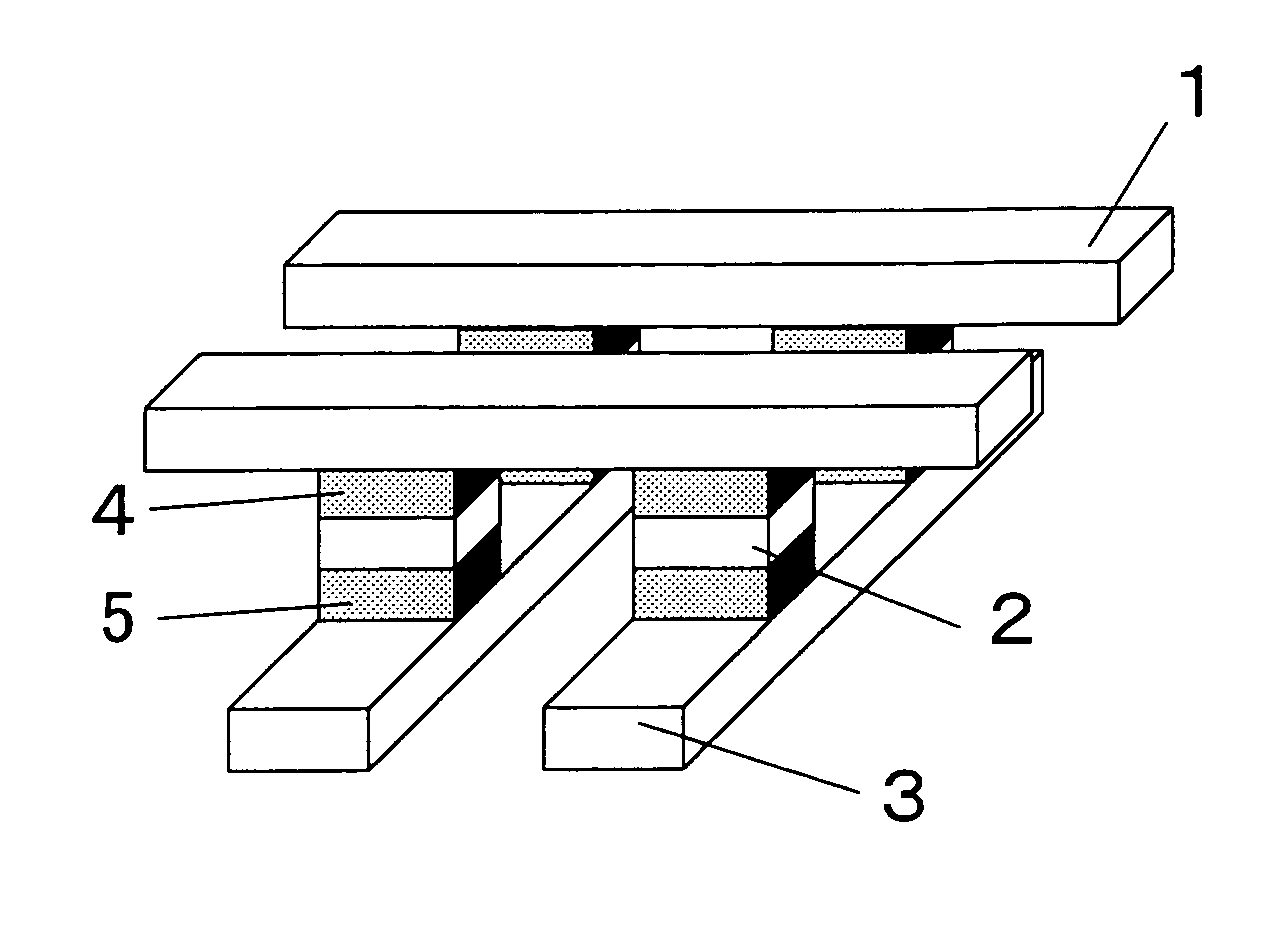
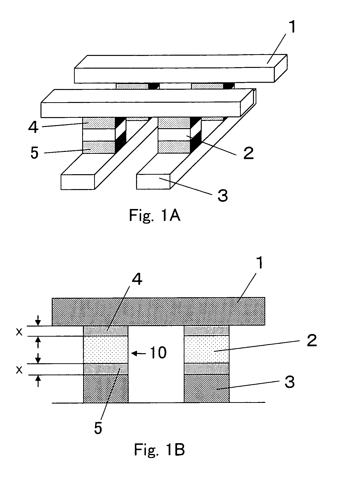
[0059]FIG. 1A is a perspective view showing a primary part of a memory array cell structure in the inventive device of the first embodiment. FIG. 1B is a cross sectional view taken along the vertical of a memory cell array shown in FIG. 1A. In the drawings, each electrical insulator provided between any two adjacent memory cells is not illustrated for simplicity.

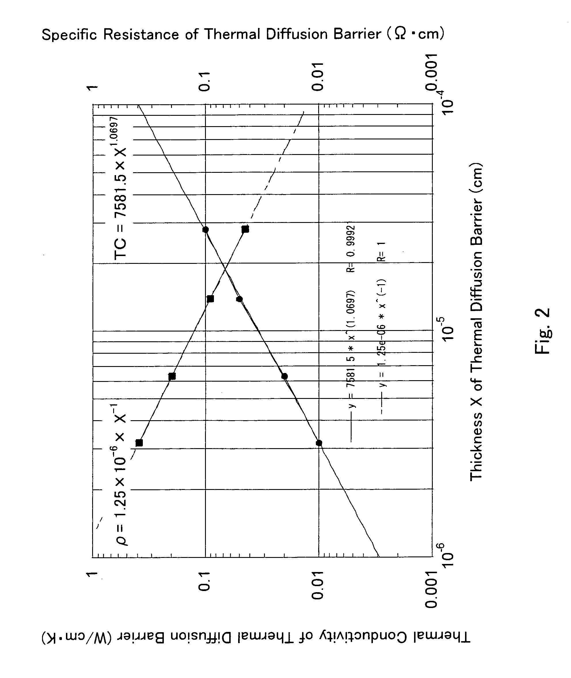
[0060]The memory cell array in the inventive device has multiple memory cells 10 arranged like a matrix in a row direction and column direction. The memory cells 10 at each column are electrically connected at one end with a thermal diffusion barrier 5 to a common word line 3. The memory cells 10 at each row are electrically connected at the other end with another thermal diffusion barrier 4 to a common bit line 1. Both the bit line 1 and the word line 3 are made of an electrically conductive wiring material. The wiring material may be aluminum (2.37 W / cm·K at thermal conductivity), copper (3.98 W / cm·K at thermal conductivit...

second embodiment

[0082]FIG. 5A is a perspective view showing a primary part of a memory cell array structure in the inventive device of the second embodiment. FIG. 5B is a cross sectional view taken along the vertical of a memory cell array shown in FIG. 5A. The second embodiment is different from the first embodiment in the shape of the thermal diffusion barriers. Hence, the second embodiment will be explained mainly in relation to the shape of the thermal diffusion barriers. In the drawings, each electrical insulator provided between any two adjacent memory cells is not illustrated for simplicity.

[0083]The memory cell array in the inventive device has multiple memory cells 20 arranged like a matrix in a row direction and column direction. The memory cells 20 at each column are electrically connected at one end with a thermal diffusion barrier 25 to a common word line 23. The memory cells 20 at each row are electrically connected at the other end with another thermal diffusion barrier 24 to a commo...

third embodiment

[0094]FIG. 7A is a perspective view showing a primary part of a memory array cell structure in the inventive device of the third embodiment. FIG. 7B is a cross sectional view taken along the vertical of a memory cell array shown in FIG. 7A. In the drawings, each electrical insulator provided between any two adjacent memory cells is not illustrated for simplicity.

[0095]The memory cell array in the inventive device has multiple memory cells 30 arranged like a matrix in a row direction and column direction. The memory cells 30 at each column are electrically connected at one end to a common word line incorporating the thermal diffusion barrier 35. The memory cells 30 at each row are electrically connected at the other end to a common bit line incorporating the thermal diffusion barrier 34. In other words, the bit line 21 and the thermal diffusion barrier 24 in the second embodiment are modified as made of one thermal diffusion barrier material. Also, the word line 23 and the thermal di...


PUM


Abstract

A nonvolatile memory device comprises memory cells, each including a variable resistor element for storing data in accordance with a change in electrical resistance due to application of electrical stress, and a thermal diffusion barrier on a thermal diffusion path, wherein the thermal diffusion barrier is capable of suppressing a change in resistance of the variable resistor element due to heat diffusion from one of two adjacent memory cells separated by an electrical insulator from each other where heat is generated by applying the electrical stress for changing the electrical resistance of the variable resistor element to the other memory cell via the thermal diffusion path including an electrically conductive wiring material higher in thermal conductivity than that of the electrical insulator.

Description

CROSS REFERENCE TO RELATED APPLICATION[0001]This Nonprovisional application claims priority under 35 U.S.C. §119(a) on Patent Application No. 2006-001645 filed in Japan on 6 Jan., 2006, the entire contents of which are hereby incorporated by reference.BACKGROUND OF THE INVENTION[0002]1. Field of the Invention[0003]The present invention relates to a nonvolatile memory device, and particularly to a nonvolatile memory device having a plurality of memory cells arranged in a matrix, each memory cell including a variable resistor element for storage of data through changing its electrical resistance with the use of electrical stress.[0004]2. Description of the Related Art[0005]Flash memories are known as nonvolatile memory devices. Such flash memories have continuously been demanded for downsizing. For the purpose, the charge in the floating gate is declined to minimize the control of threshold voltage or the length of channels is decreased to minimize the withstanding pressure between so...

Claims


Application Information

Patent Timeline
Patent Type & Authority Patents(United States)
IPC IPC(8): H01L29/06H01L47/00
CPCG11C13/0007G11C13/0033H01L27/2409H01L27/2463G11C7/04G11C2213/51G11C2213/72H01L45/04H01L45/06H01L45/1233H01L45/128H01L45/144H01L45/147H01L45/1675H10B63/20H10B63/80H10N70/231H10N70/20H10N70/861H10N70/826H10N70/8828H10N70/8836H10N70/063
Inventor SUGITA, YASUHIROTAMAI, YUKIO
Owner XENOGENIC DEV LLC
Why Eureka
Try Eureka