SET and SEGR resistant delay cell and delay line for Power-On Reset circuit applications

a technology of delay cell and segr, which is applied in the direction of pulse manipulation, pulse technique, electrical apparatus, etc., can solve the problems of affecting the performance of the integrated circuit into which the por circuit was incorporated, damage to the circuit, and may not be optimum for circuits used in space environments, so as to increase the circuit area, improve the effect of performance and increase the manufacturing cos

Active Publication Date: 2010-06-08
CAES COLORADO SPRINGS LLC
View PDF7 Cites 4 Cited by
  • Summary
  • Abstract
  • Description
  • Claims
  • Application Information

AI Technical Summary

Benefits of technology

[0004]According to the present invention, a delay line appropriate for use in a POR circuit or other integrated circuits in a space environment combines three separate circuit techniques to improve performance without unnecessarily increasing circuit area or adding to manufacturing costs when compared to a simple inverter delay line. The delay line of the present invention uses the selective placement of capacitors throughout the delay line, one-sided current starving, and the incorporation of one-sided Schmitt trigger circuits.
[0005]The actual delay element, a capacitor, is placed only on odd stages of the delay line, and the capacitors are completely discharged during normal operation. This substantially eliminates the threat of a SEGR related event damaging the part or producing a spurious reset signal. This is because the energy a heavy ion requires to cause a rupture is inversely proportional to the square of the voltage across the capacitor. With a voltage at or near zero volts, the required ion energy for rupture is beyond that found in any known space environment.
[0006]Since the delay element, the capacitor, is current starved from only one side, transient pulses are substantially eliminated after every even stage in the delay chain, preventing SET event disruption. Transient pulses are reduced due to the asymmetrical use of current starving in the delay chain.
[0007]The reduction in the transient pulses provided by the current starving technique is reinforced by the use of “half Schmitt” trigger circuits in the delay line. A typical delay line attenuates the width of a transient pulse about one-half of its width through each even / odd pair of delay stages in the delay chain. Through the use of the half Schmitt trigger circuit in the present invention, a transient pulse is reduced in width when passing through a single even / odd pair of delay stages. Since the response of the next transistor in the delay line of the present invention is weakened due to current starving and heavy load capacitance, a spurious pulse caused by a heavy ion with an LET (“Linear Energy Transfer”) of even 100 Mev-cm2 / mg are eliminated after only one even / odd chain pair of delay stages.
[0008]Using the half Schmitt trigger circuit scheme of the present invention, the capacitors in the odd stages of the delay chain are almost completely discharged before passing along a reset signal, thus making the most efficient use of capacitor area. Additionally, the one-sided current starved configuration of the present invention can be adjusted to provide a very minimal discharge current thus further maximizing the delay available from a given capacitive element.

Problems solved by technology

While an inverter delay line can be simply designed and manufactured, and is a cost effective solution for a wide number of applications, such a solution may not be optimum for circuits used in a space environment.
A space environment is subject to radiation not found in terrestrial applications that can damage circuits and affect performance.
If the inverter delay line were incorporated into a POR circuit, for example, a SET event could cause the POR circuit to send out a spurious reset signal, which would disrupt the performance of the integrated circuit into which the POR circuit was incorporated.
Similarly, a SEGR event could also send out a spurious reset signal, but, in addition, could fatally damage the POR circuit and cause the entire integrated circuit into which the POR circuit was incorporated to become permanently inoperable.

Method used


Image

  • SET and SEGR resistant delay cell and delay line for Power-On Reset circuit applications
  • SET and SEGR resistant delay cell and delay line for Power-On Reset circuit applications
  • SET and SEGR resistant delay cell and delay line for Power-On Reset circuit applications

Examples


Embodiment Construction

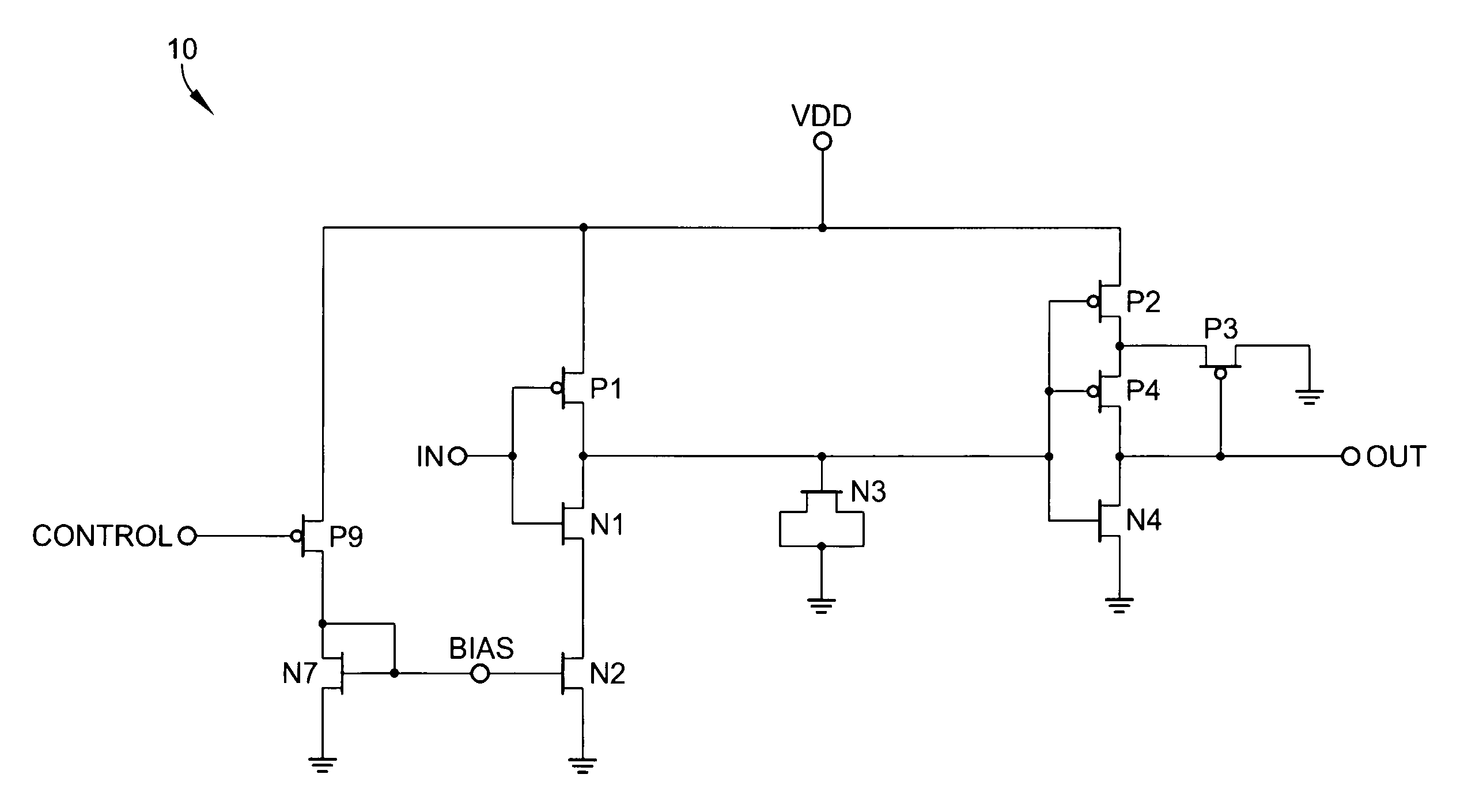
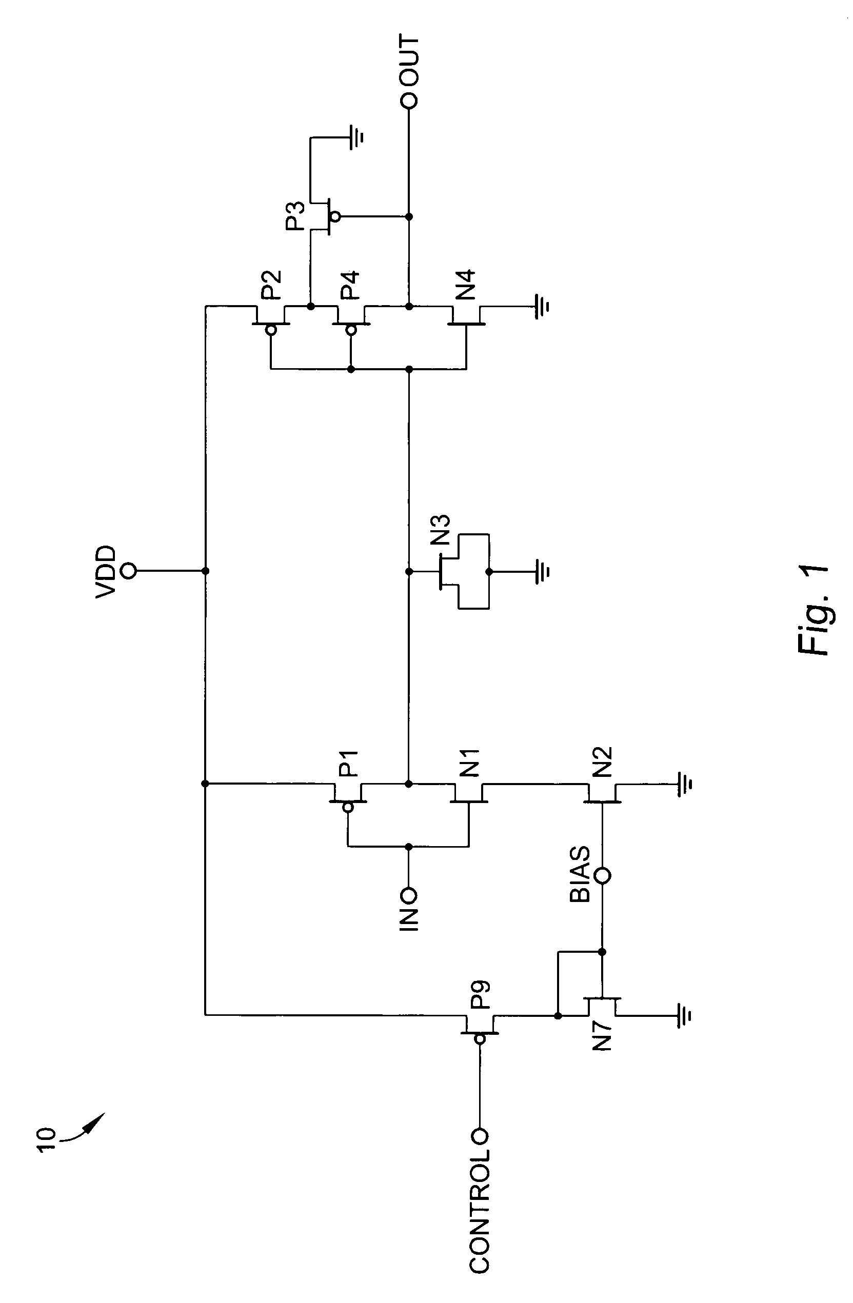
[0014]Referring now to FIG. 1, an SET and SEGR resistant delay cell 10 includes a delay input node marked “IN” and a delay output node marked “OUT”. A one-sided current starved inverting input section (odd delay stage) has an input coupled to the delay input, and an output. A capacitor is coupled between the output of the input section and ground. A half-Schmitt trigger circuit (even delay stage) has an input coupled to the output of the input section, and an output coupled to the delay output.

[0015]The input section, which is also referred to as an odd delay stage, includes a P-channel transistor P1 having a source coupled to VDD, a gate coupled to the input, and a drain coupled to the output. A first N-channel transistor N1 has a source, a gate coupled to the input, and a drain coupled to the output. A second N-channel transistor N2 has a source coupled to ground, a gate for receiving a bias voltage at a node marked “BIAS”, and a drain coupled to the source of the first N-channel ...


PUM


Abstract

A delay line appropriate for use in a POR circuit or other integrated circuit in a space environment combines three separate circuit techniques to improve performance without unnecessarily increasing circuit area or adding to manufacturing costs when compared to a simple inverter delay line. The delay line of the present invention uses the selective placement of capacitors throughout the delay line, one-sided current starving, and the incorporation of one-sided Schmitt trigger circuits. Performance of the delay line is substantially immune to SEGR events (“Single Event Gate Rupture”) and SET events (“Single Event Transients”). Spurious signals produced by SEGR and SET events are quickly and substantially attenuated.

Description

BACKGROUND OF THE INVENTION[0001]It is known in the art that a delay cell can simply be constructed of a single inverter and a capacitive delay element. Similarly, an entire delay line can be constructed of a chain of inverter delay cells, wherein the output of an inverter delay cell is coupled to the output of the next inverter delay cell. Delay lines are widely used in a great number of integrated circuit applications. They are used, for example, in POR (“Power On Reset”) circuits.[0002]While an inverter delay line can be simply designed and manufactured, and is a cost effective solution for a wide number of applications, such a solution may not be optimum for circuits used in a space environment. A space environment is subject to radiation not found in terrestrial applications that can damage circuits and affect performance. Using a standard inverter delay line circuit in a space environment is not advised because it would be subject to SEGR events (“Single Event Gate Rupture”) a...

Claims


Application Information

Patent Timeline
Patent Type & Authority Patents(United States)
IPC IPC(8): H03H11/26
CPCH03H11/26
Inventor VON THUN, MATTHEW
Owner CAES COLORADO SPRINGS LLC
Why Eureka
Try Eureka