Waveguide to microstrip line transition having a conductive footprint for providing a contact free element

a technology of contact free elements and waveguides, which is applied in the direction of electrical devices, multiple-port networks, coupling devices, etc., can solve the problems of complex and inflexible components described above, and achieve the effect of limiting the leakage of electrical fields and preventing short-circuits

Inactive Publication Date: 2010-06-29
THOMSON LICENSING SA
View PDF6 Cites 8 Cited by
  • Summary
  • Abstract
  • Description
  • Claims
  • Application Information

AI Technical Summary

Benefits of technology

[0008]The present invention therefore proposes a new type of contact-free transition between a waveguide structure and a structure realized using microstrip technology. This transition is simple to realize and allows wide manufacturing and assembly tolerances. Moreover, the transition of the present invention is compatible with the SMD mounting technology.
[0013]According to a second embodiment, the securing flange is realized in the extension of the waveguide. In this case, the microstrip line preferably terminates in a capacitive probe and the cavity has a depth between λ / 4 and λ / 2 where λ corresponds to the guided wavelength in the waveguide. To prevent electrical leakage, the conductive footprint is realized on the substrate to enable the connection with a C-shaped flange, the opening between the branches of the C-shaped footprint being dimensioned to limit the leakage of electrical fields while preventing short-circuits.

Problems solved by technology

In all cases, the embodiments described above are complex and inflexible.

Method used


Image

  • Waveguide to microstrip line transition having a conductive footprint for providing a contact free element
  • Waveguide to microstrip line transition having a conductive footprint for providing a contact free element
  • Waveguide to microstrip line transition having a conductive footprint for providing a contact free element

Examples


Embodiment Construction

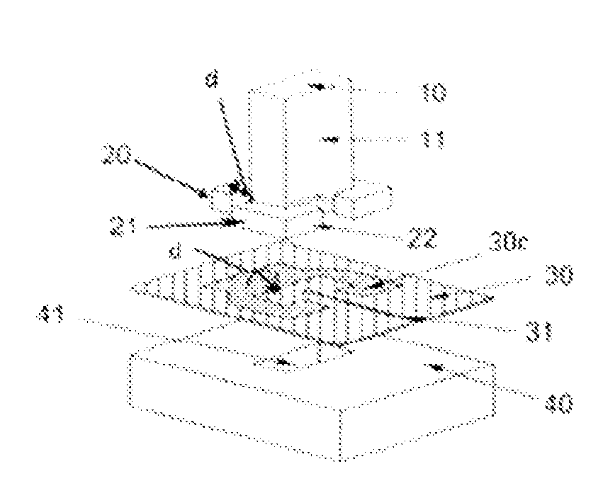
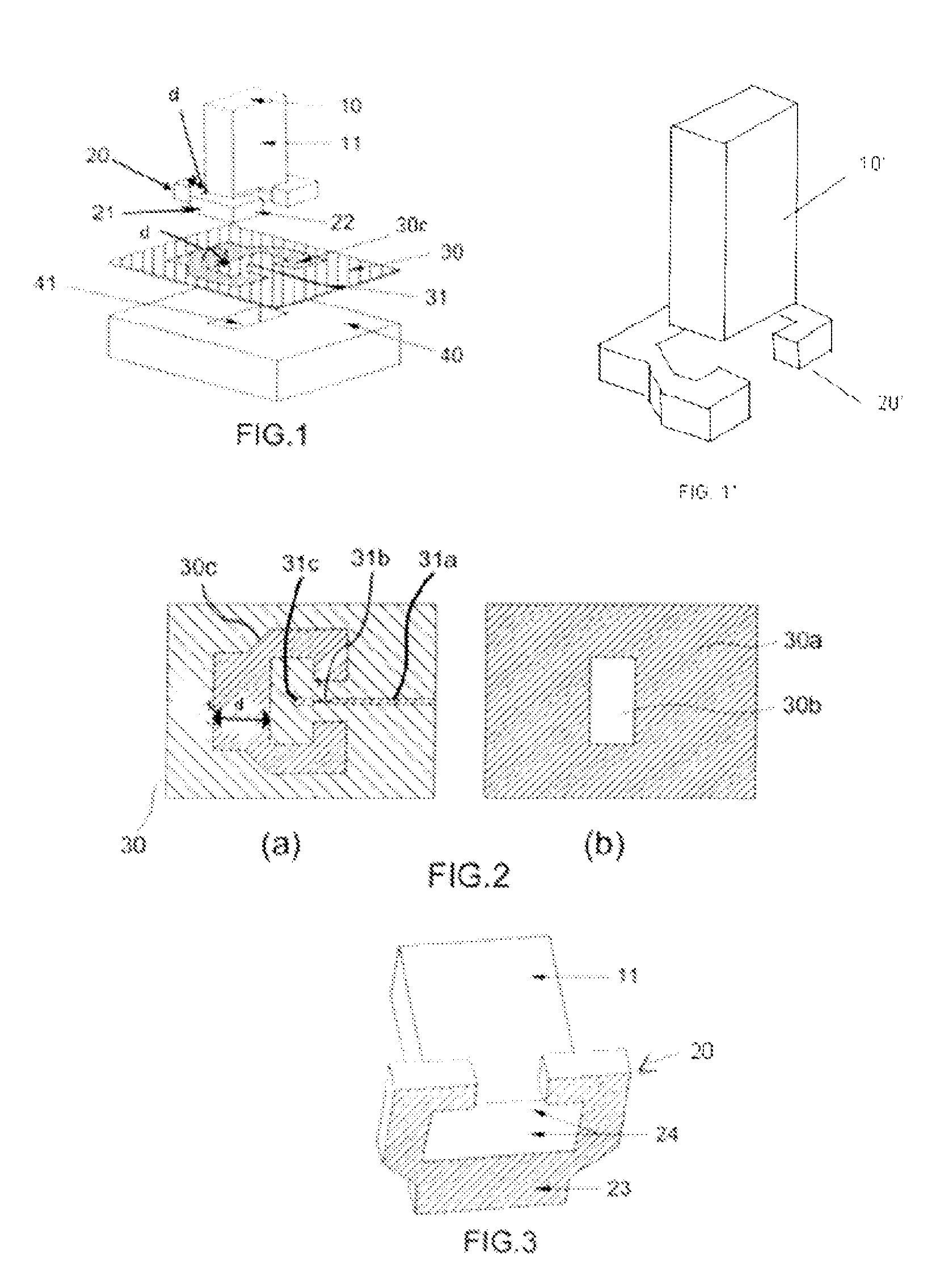
[0037]A first description with reference to FIGS. 1 to 4 will be made for a first embodiment of a transition element between a waveguide circuit and a microstrip line realized on a dielectric substrate.

[0038]As shown diagrammatically in FIG. 1, which relates to an exploded view of the transition element, the reference 10 diagrammatically shows a rectangular waveguide. This waveguide is preferably realized in a synthetic material, more particularly in foam with a permittivity noticeably similar to that of air. The rectangular block of foam is metallized, as referenced by 11, on all the external surfaces so as to realize a microwave waveguide.

[0039]As shown particularly in FIG. 1, a flange 20, which presents a noticeable “C” shape, is realized at one end of the guide 10, preferably at the same time as the foam technology waveguide. This flange 20 surrounds the rectangular extremity of the guide 10 on its two smaller sides 21 and on one of its large sides while the other large side has...


PUM


Abstract

The present invention relates to an element of transition between a waveguide and a transition line on a substrate. The element of transition comprises a securing flange on the substrate, the flange being dimensioned so that at least, in the direction microstrip line, the width d of the flange is selected in such a manner as to shift the resonant modes away from the useful band. The invention is used particularly for circuits using SMD techniques at millimeter frequencies.

Description

[0001]The present invention relates to a transition element between a microstrip technology line circuit and a waveguide circuit, more particularly a contact-free transition between a microstrip technology feeding line and a rectangular waveguide realized by using metallized foam based technology.BACKGROUND OF THE INVENTION[0002]Radio communication systems that can transmit high bit-rates are currently experiencing strong growth. The systems being developed, particularly the point-to-multipoint systems such as the LMDS (Local Multipoint Distribution System) systems and WLAN (Wireless Local Area Network) wireless systems, operate at increasingly higher frequencies, namely in the order of several tens of Giga-Hertz. These systems are complex but must be realized at increasingly lower costs due to their use by consumers. There are now technologies such as LTCC (Low Temperature Cofired Ceramic) or HTCC (High Temperature Cofired Ceramic) technologies that enable devices integrating passi...

Claims


Application Information

Patent Timeline
Patent Type & Authority Patents(United States)
IPC IPC(8): H01P5/107H01P1/207
CPCH01P5/107
Inventor TONG, DOMINIQUE LO HINEMINARD, PHILIPPENICOLAS, CORINNELOUZIR, ALITHEVENARD, JULIANCOUPEZ, JEAN-PHILIPPEPERSON, CHRISTIAN
Owner THOMSON LICENSING SA
Why Eureka
Try Eureka