Capacitor built-in interposer and method of manufacturing the same and electronic component device

a technology of built-in interposers and capacitors, which is applied in the direction of fixed capacitor details, printed circuit non-printed electric components association, and semiconductor/solid-state device details, etc., can solve the problems of difficult wiring routes, circuit design restrictions, and insufficient effect of decoupling capacitors, etc., to achieve easy manufacturing, easy construction, and large design margin

Inactive Publication Date: 2010-07-13
SHINKO ELECTRIC IND CO LTD
View PDF19 Cites 12 Cited by
  • Summary
  • Abstract
  • Description
  • Claims
  • Application Information

AI Technical Summary

Benefits of technology

[0019]In this manner, in the capacitor built-in interposer of the present invention, the first and second electrodes of the capacitor provided to pass through the base resin layer can be connected directly to the wiring substrate and the semiconductor chip. Therefore, unlike the prior art, there is no need to route around the wiring connected to the capacitor in the wiring substrate upon connecting the wiring to the semiconductor chip. As a result, the inductance generated between the capacitors and the semiconductor chip can be reduced, and thus the capacitor built-in interposer can perform enough performances as the decoupling capacitor for the semiconductor chip that operates at a high speed. In addition, since this capacitor built-in interposer has the through electrode serving as the conductive path, such interposer can be used equally to the common interposer.
[0020]Also, there is no need to mount the capacitor component on the wiring substrate, or to build in the capacitor into the wiring substrate. Therefore, the electronic component device can formed with a simple structure and also a margin of design of the electronic component device can be widened.
[0024]The capacitor built-in interposer of the present invention can be easily manufactured by using the above manufacturing method. Also, the through electrode and the resistor portion as well as the capacitors can be easily built in on the basis of forming the plating opening portions in portions on another metal posts and then forming the metal bumps after the capacitor is formed.

Problems solved by technology

In some cases, an effect of the decoupling capacitor cannot be sufficiently achieved.
Also, in the prior art, such problems have arisen that it is difficult to change the wiring routes because positions of the connection terminals of the capacitor component are restricted, and a circuit design is restricted and a margin of design is small because the die attaching tape must be used, and others.
As a result, the similar problems have arisen.

Method used


Image

  • Capacitor built-in interposer and method of manufacturing the same and electronic component device
  • Capacitor built-in interposer and method of manufacturing the same and electronic component device
  • Capacitor built-in interposer and method of manufacturing the same and electronic component device

Examples


first embodiment

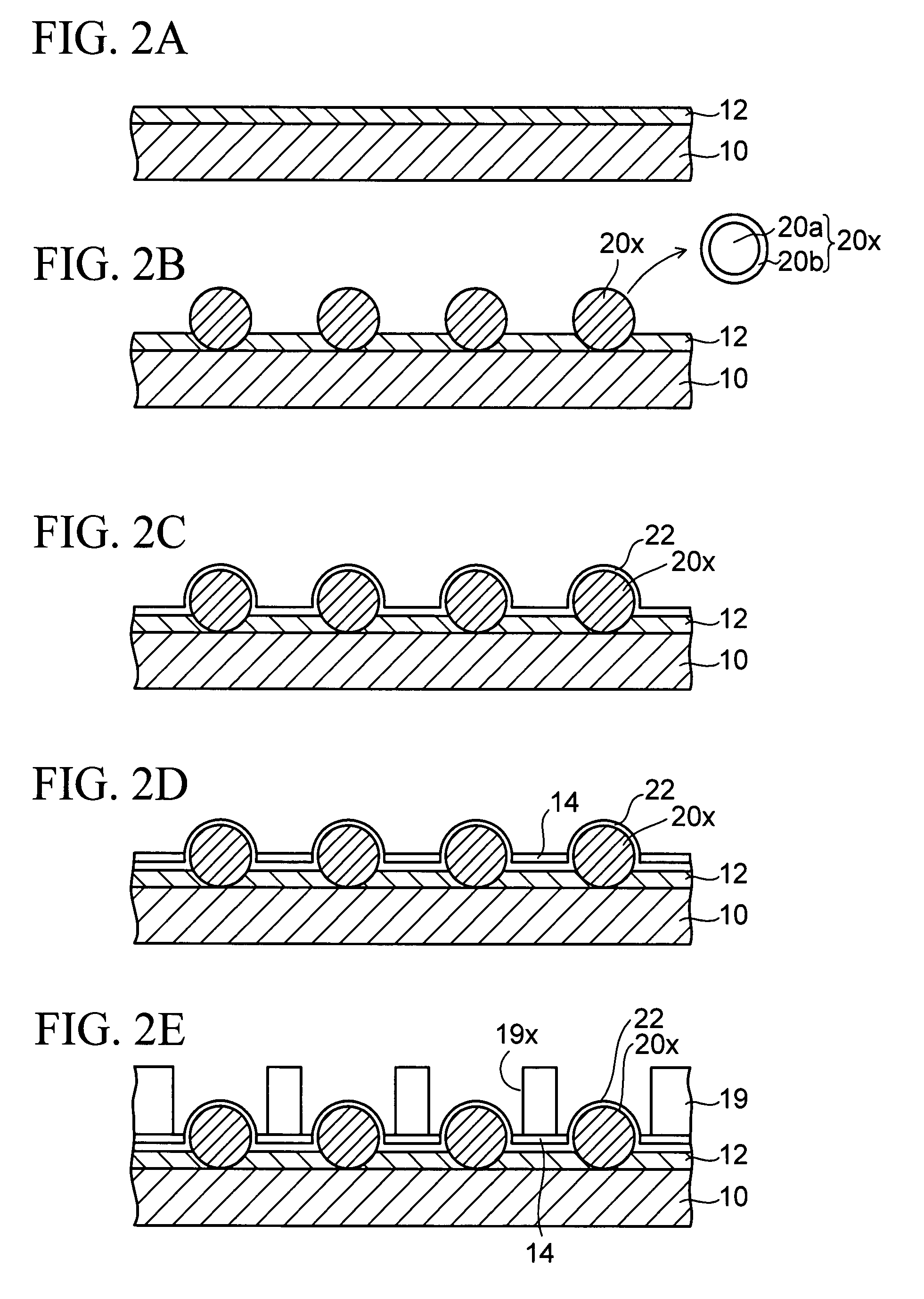
[0037]FIGS. 2A to 2K are sectional views showing a method of manufacturing a capacitor built-in interposer according to a first embodiment of the present invention, and FIG. 3 is a sectional view showing similarly the capacitor built-in interposer.

[0038]In the method of manufacturing a capacitor built-in interposer according to the present embodiment, as shown in FIG. 2A, first, a copper plate 10 as a metal supporting body is prepared, and a tin layer 12 acting as a flexible metal layer is formed by plating a tin on the copper plate 10. A thickness of the copper plate 10 is 0.3 to 0.4 mm, and a film thickness of the tin layer 12 is almost 60 μm.

[0039]Then, as shown in FIG. 2B, spherical conductors 20x a diameter of each of which is about 5 to 200 μm are prepared. The spherical conductor 20x is constructed by covering an outer surface of a copper ball 20a with a gold layer 20b. As the spherical conductor 20x, a ball constructed by covering an outer surface of each of various metal ba...

second embodiment

[0061]FIGS. 6A to 6O are sectional views showing a method of manufacturing a capacitor built-in interposer according to a second embodiment of the present invention, and FIG. 7 is a sectional view showing the capacitor built-in interposer similarly. In the foregoing first embodiment, spherical capacitors C are formed from all spherical conductor 20x on the basis of arranging a plurality of spherical conductors 20x on the tin layer 12 formed on the copper plate 10 with area array type. Normally, the semiconductor chip 45 is equipped with signal lines, etc. Therefore, in the first embodiment, the conductive paths such as the signal lines, and the like of the semiconductor chip 45 are ensured by providing the bumps 45a separately between the semiconductor chip 45 and the wiring substrate 30.

[0062]A feature of the second embodiment resides in that through electrodes serving as conductive paths such as the signal lines, or the like and resistor portions in addition to the capacitors are ...

third embodiment

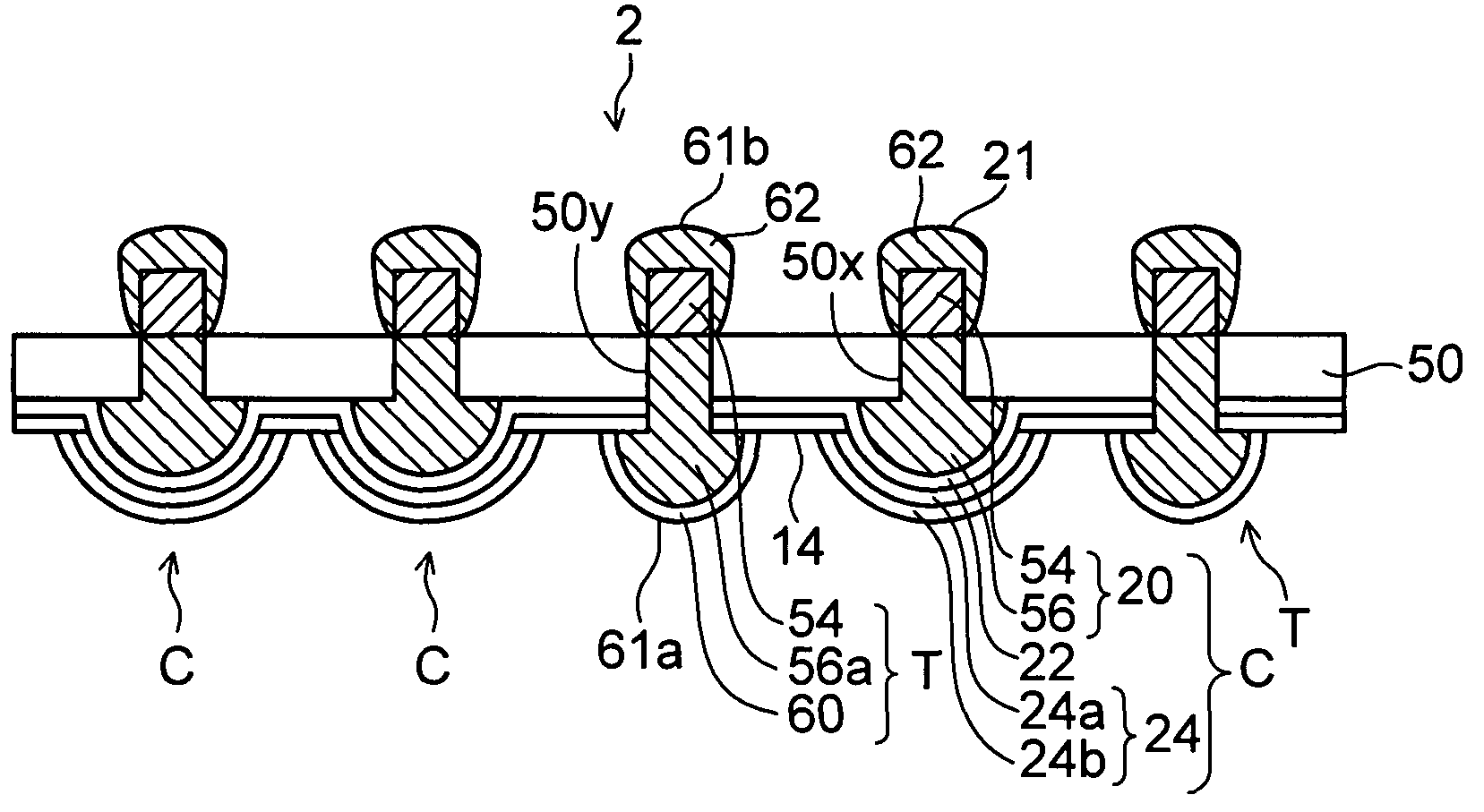
[0099]FIGS. 10A to 10G are sectional views showing a method of manufacturing a capacitor built-in interposer according to a third embodiment of the present invention. A feature of the third embodiment resides in that the solder layer is utilized finally as the coating layer for the copper post on the basis of filling the solder layer in concave portions provided in the copper plate and then embedding the copper posts in the solder layers. In the third embodiment, detailed explanation of the same steps as those in the second embodiment will be omitted herein.

[0100]In the manufacturing method of the third embodiment, as shown in FIGS. 10A and 10B, the copper plate 10 as a metal supporting body is prepared, and a resist 11 having opening portions 11x is formed on the copper plate 10. Then, concave portions 10x are formed in the copper plate 10 by wet-etching the copper plate 10 through the opening portions 11x in the resist 11. Then, as shown in FIG. 10C, the solder layers 62 are forme...


PUM

PropertyMeasurementUnit
thicknessaaaaaaaaaa
thicknessaaaaaaaaaa
diameteraaaaaaaaaa

Abstract

A capacitor built-in interposer of the present invention, includes a base resin layer, a capacitor first electrode provided to pass through the base resin layer and having projection portions projected from both surface sides of the base resin layer respectively whereby the projection portion on one surface side of the base resin layer serves as a connection portion, a capacitor dielectric layer for covering the projection portion of the first electrode on other surface side of the base resin layer, and a capacitor second electrode for covering the dielectric layer, wherein a plurality of capacitors each constructed by the first electrode, the dielectric layer, and the second electrode are arranged and aligned in a lateral direction in a state that the capacitors are passed through the base resin layer.

Description

CROSS-REFERENCE TO RELATED APPLICATIONS[0001]This application is based on and claims priority of Japanese Patent Application No. 2006-214205 filed on Aug. 7, 2006, the entire contents of which are incorporated herein by reference.BACKGROUND OF THE INVENTION[0002]1. Field of the Invention[0003]The present invention relates to a capacitor built-in interposer and a method of manufacturing the same and an electronic component device and, more particularly, a capacitor built-in interposer applicable to an interposer used to connect a semiconductor chip and a wiring substrate and a method of manufacturing the same and an electronic component device utilizing the same.[0004]2. Description of the Related Art[0005]In the prior art, there is the electronic component device constructed by mounting the semiconductor chip on the wiring substrate in which the decoupling capacitor is built. As shown in FIG. 1, in an example of such electronic component device, first wiring layers 100 are embedded ...

Claims


Application Information

Patent Timeline
Patent Type & Authority Patents(United States)
IPC IPC(8): H05K1/16H01L23/12H01L23/32
CPCH01G4/33H01G4/38H01L21/486H01L23/49827H01L23/50H05K1/162H01L23/642H01G4/236Y10T29/435H01L2924/09701H05K2201/0367H05K2201/09763H05K2201/10378H01L2224/16225H01L2224/16268H01L2224/81192H01L2924/15311H01L2924/19041H01L2924/19103
Inventor MASHINO, NAOHIRO
Owner SHINKO ELECTRIC IND CO LTD
Why Eureka
Try Eureka