Capacitor built-in interposer and method of manufacturing the same and electronic component device
a technology of built-in interposers and capacitors, which is applied in the direction of capacitor manufacturing, fixed capacitor details, printed circuit non-printed electric components association, etc., can solve the problems of difficult wiring routes, circuit design restrictions, and insufficient effect of decoupling capacitors, etc., to achieve easy manufacturing, easy construction, and large design margin
- Summary
- Abstract
- Description
- Claims
- Application Information
AI Technical Summary
Benefits of technology
Problems solved by technology
Method used
Image
Examples
first embodiment
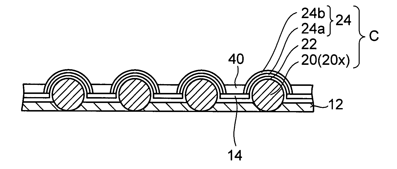
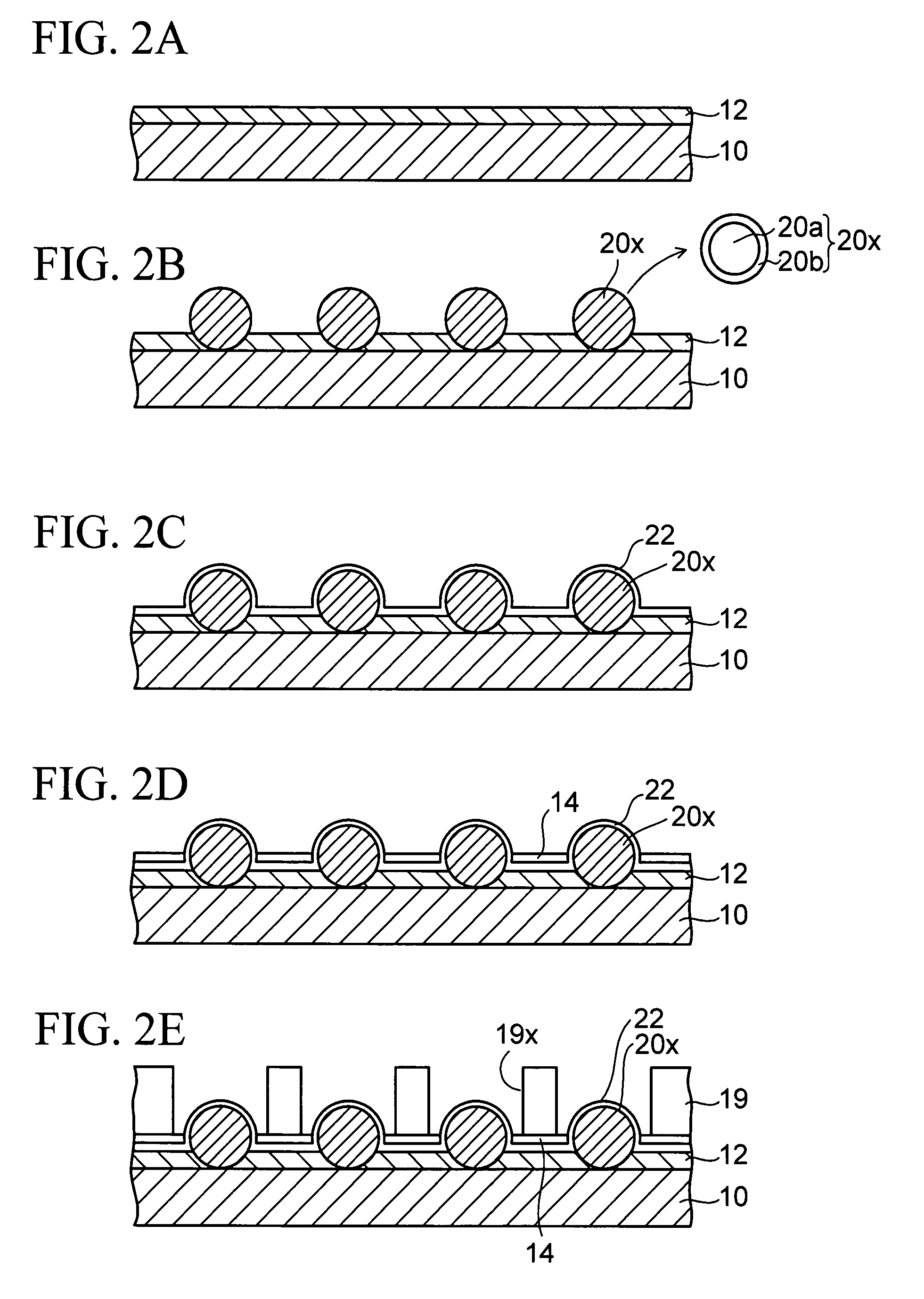
[0037]FIGS. 2A to 2K are sectional views showing a method of manufacturing a capacitor built-in interposer according to a first embodiment of the present invention, and FIG. 3 is a sectional view showing similarly the capacitor built-in interposer.
[0038]In the method of manufacturing a capacitor built-in interposer according to the present embodiment, as shown in FIG. 2A, first, a copper plate 10 as a metal supporting body is prepared, and a tin layer 12 acting as a flexible metal layer is formed by plating a tin on the copper plate 10. A thickness of the copper plate 10 is 0.3 to 0.4 mm, and a film thickness of the tin layer 12 is almost 60 μm.
[0039]Then, as shown in FIG. 2B, spherical conductors 20x a diameter of each of which is about 5 to 200 μm are prepared. The spherical conductor 20x is constructed by covering an outer surface of a copper ball 20a with a gold layer 20b. As the spherical conductor 20x, a ball constructed by covering an outer surface of each of various metal ba...
second embodiment
[0061]FIGS. 6A to 6O are sectional views showing a method of manufacturing a capacitor built-in interposer according to a second embodiment of the present invention, and FIG. 7 is a sectional view showing the capacitor built-in interposer similarly. In the foregoing first embodiment, spherical capacitors C are formed from all spherical conductor 20x on the basis of arranging a plurality of spherical conductors 20x on the tin layer 12 formed on the copper plate 10 with area array type. Normally, the semiconductor chip 45 is equipped with signal lines, etc. Therefore, in the first embodiment, the conductive paths such as the signal lines, and the like of the semiconductor chip 45 are ensured by providing the bumps 45a separately between the semiconductor chip 45 and the wiring substrate 30.
[0062]A feature of the second embodiment resides in that through electrodes serving as conductive paths such as the signal lines, or the like and resistor portions in addition to the capacitors are ...
third embodiment
[0099]FIGS. 10A to 10G are sectional views showing a method of manufacturing a capacitor built-in interposer according to a third embodiment of the present invention. A feature of the third embodiment resides in that the solder layer is utilized finally as the coating layer for the copper post on the basis of filling the solder layer in concave portions provided in the copper plate and then embedding the copper posts in the solder layers. In the third embodiment, detailed explanation of the same steps as those in the second embodiment will be omitted herein.
[0100]In the manufacturing method of the third embodiment, as shown in FIGS. 10A and 10B, the copper plate 10 as a metal supporting body is prepared, and a resist 11 having opening portions 11x is formed on the copper plate 10. Then, concave portions 10x are formed in the copper plate 10 by wet-etching the copper plate 10 through the opening portions 11x in the resist 11. Then, as shown in FIG. 10C, the solder layers 62 are forme...
PUM
| Property | Measurement | Unit |
|---|---|---|
| thickness | aaaaa | aaaaa |
| thickness | aaaaa | aaaaa |
| diameter | aaaaa | aaaaa |
Abstract
Description
Claims
Application Information


