[0043]The basic concept of the 3-D structure in accordance with the invention is illustrated in FIG. 8. In FIG. 8, memory cells (in a rectangular matrix array for clarity of illustration, similar to that of FIGS. 2 and 3) are illustrated in an isometric view with word lines running from upper left to lower right and bit line pairs running from upper right to lower left in registration with the memory cells. The array of memory cells is depicted as being formed on (or in) ground plane 80 which is or is parallel to a substrate or chip surface. Peripheral or support circuits such as sense amplifiers (e.g. SA) and / or address decoders (e.g. AD) are formed in at least a second plane different from that defined by the chip or substrate carrying the memory cells 44. In general, a single second plane will be sufficient to carry an adequate number of peripheral or support circuits to realize the meritorious effects of the invention, as will be discussed in greater detail below, although a third, fourth of more further additional planes could be added if desired.
[0044]It is very important to a full appreciation of the invention that in a configuration such as that depicted in FIG. 8, sense amplifier connections to bit lines or bit line pairs or connections thereto (e.g. 48 through local evaluation circuits 44) may be made at any point along the length of the bit lines in a second plane and need not be confined to the central portion of the array, as is generally a feature of single plane memory layouts as alluded to above. By the same token, address decoders and / or word line drivers may be placed at any location in a second plane along the entire length of any particular word line. The importance of this feature of the invention in addition to allowing more area of a second or further plane to be used for support circuits is that it also facilitates using a greater fraction of chip area in a second or further plane as well as making connections from any location in the second or further plane to the ground plane circuits without causing significant increase in connection length. Several preferred ways of exploiting this feature of the invention will be discussed in greater detail below. Further, since support / peripheral circuits (and selectors for allowing sharing between them and the bit lines) can thus be freely located in or on the second or further plane, there is no restriction due to required position or connection length on the number of support or peripheral circuits which may be formed, and, ideally, the sense amplifiers and / or local evaluation circuits may be sufficiently increased in number that sharing of sense amplifiers for a plurality of bit lines or bit line pairs is significantly reduced or eliminated along with the potential for elimination of the half-select mode in a manner which is much more simple than is possible when sense amplifiers are shared. Even if sense amplifiers must be shared, the number of bit lines serviced by each sense amplifier can be reduced to reduce the effects of sharing on potential cell instability and which is further reduced by the provision of local evaluation circuits. By the same token, the SRAM array density can be maintained or improved without sacrificing or compromise of functionality and performance while more chip area for a chip of given size can be used for the memory cell array. Thus, several possible embodiments of the invention are possible such as forming the local evaluation circuits 44 in the same plane with the memory cells and sense amplifiers 46 removed to a second plane, forming both the local evaluation circuits in a second plane (making essentially the full area of the ground plane chip available for memory cells) or populating the second plane principally or fully with local evaluation circuits 44 (which are, in any case, a form of sense amplifiers) and forming sense amplifiers 46 or at least a portion of them on yet another plane or chip.
[0045]It should also be noted in connection with FIG. 8 that the length of connections between the planes is not significantly increased since the connections between planes can be made at essentially arbitrary locations and, if the respective support circuits are positioned above the word lines or bit lines to which they correspond (which is easily accomplished since the individual sense amplifiers and word line drivers are fungible and the word line decoder can be designed to have suitably distributed outputs), the connection length can be held to the sum of the respective thicknesses of the semiconductor devices and their in-plane connections, the thickness of passivation layers on the respective substrates and the thickness of the bond between the substrates. This sum of thicknesses may be held to approximately the thickness of the active layer of an SOI substrate by a number of techniques well-understood in the art and as will be detailed below.
[0046]FIG. 9 is a cross-section taken at section Z-Z′ of the memory stricture illustrated in plan view in FIG. 7. Local connection in the memory cells can be made using CA and MCBAR structures discussed above which are well-understood in the art. These connections include PC to RX connections, RX to metal layer connections PC to metal layer connections and the like. The interconnections between the respective memory cells and local evaluation circuits / sense amplifiers can be made using the first metal layer (M1) between the two planes. This 3-D memory device architecture thus allows any desired portion of the support / peripheral circuits to be placed in a second or further planes, such as placing the local evaluation circuits 44 (which function as a type of sense amplifier as well as providing isolation) in a second plane with reduction of the number of memory cells shared by each local evaluation circuit and with simplified sense amplifiers 46 in increased numbers in either the second plane or a third plane with selection circuits between the local evaluation circuits 44 and sense amplifiers 46 in either the second or third plane.
[0047]Placing the memory cells and at least a portion of the support or peripheral circuits in different planes also has meritorious effects during manufacture by allowing the memory structures and peripheral / support circuit structures (which usually involve transistors of very different designs and sizes) to be manufactured separately with fully decoupled process sequences applied to different wafers as shown as 1010 and 1020 of FIG. 10; a preferred process sequence for which will be detailed below in connection with FIGS. 14-18. Perhaps more importantly, however, such separate fabrication allows separate test and functionality verification of the memory cells and peripheral / support circuits before the planes are bonded together (which thereafter restricts testing probe access and / or access for any repairs or engineering changes which can enhance manufacturing yield) or wired together (which thereafter complicates interpretation of test results and fault location) as shown at steps 1030, 1040 and 1050 of FIG. 10. These steps allow much enhanced manufacturing yield and confidence level in the operability and quality of the completed SRAM. After such testing and associated processes, the bonded integrated circuit planes may be completed by resuming standard back end of line (BEOL) processes as shown at 1060, 1070 and 1080 of FIG. 10.
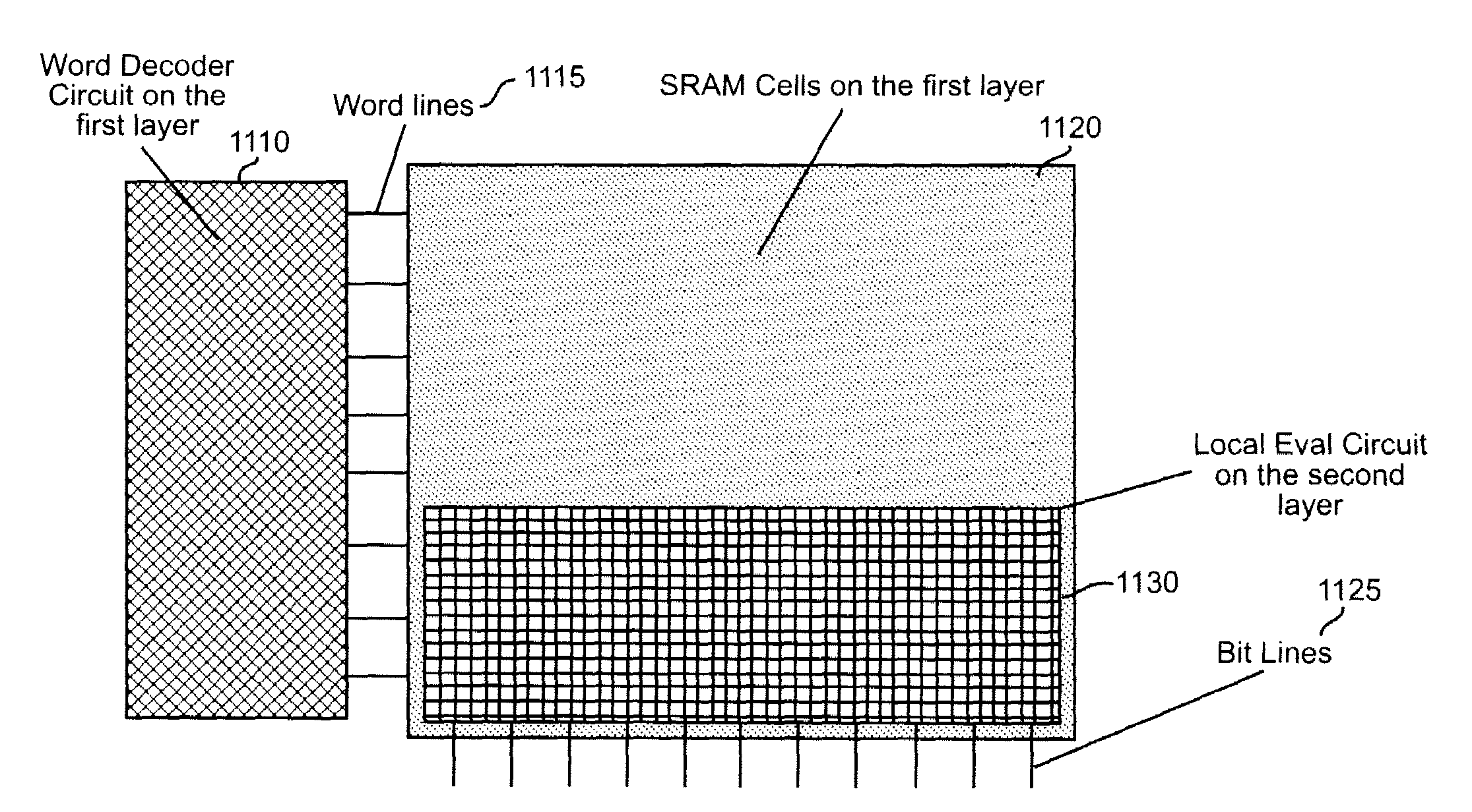
[0048]Referring now to FIG. 11, a layout for a SRAM formed in a single plane is schematically illustrated in plan view. Since this depiction includes local evaluation circuits rather than sense amplifiers at 1130, no portion of FIG. 11 is admitted to be prior art in regard to the invention. In order to select a row in which a memory cell of interest is included, a word decoder circuit 1110 (generally including a word line driver circuit) is provided to apply a selection voltage to one of the word lines 1115 connected to the memory cell array 1120 the application of a selection voltage to a word line connects a row of memory cells to bit line 1125 pairs respectively corresponding to the individual memory cells in the selected row as discussed above in connection with FIG. 1 and thus to the local evaluation circuits 1130 as discussed above in connection with FIG. 4. It can be appreciated that such a configuration severely limits the area which can be allocated to memory cells and, while word line and bit line lengths are substantially minimized, the length and capacitance thereof is significant.

