Method of manufacturing microneedle structures using photolithography
- Summary
- Abstract
- Description
- Claims
- Application Information
AI Technical Summary
Benefits of technology
Problems solved by technology
Method used
Image
Examples
Embodiment Construction
[0047]Reference will now be made in detail to the present preferred embodiment of the invention, an example of which is illustrated in the accompanying drawings, wherein like numerals indicate the same elements throughout the views.
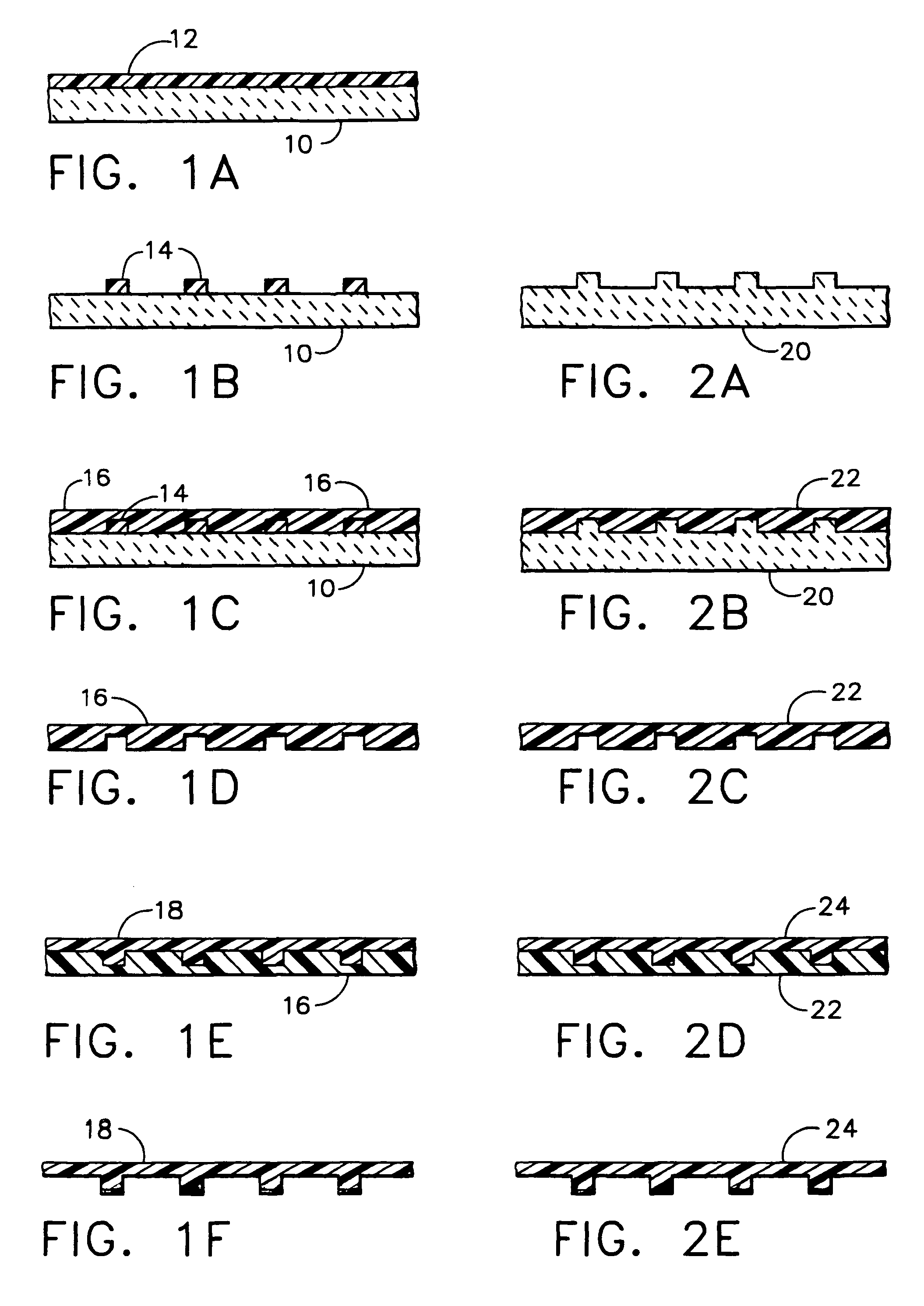
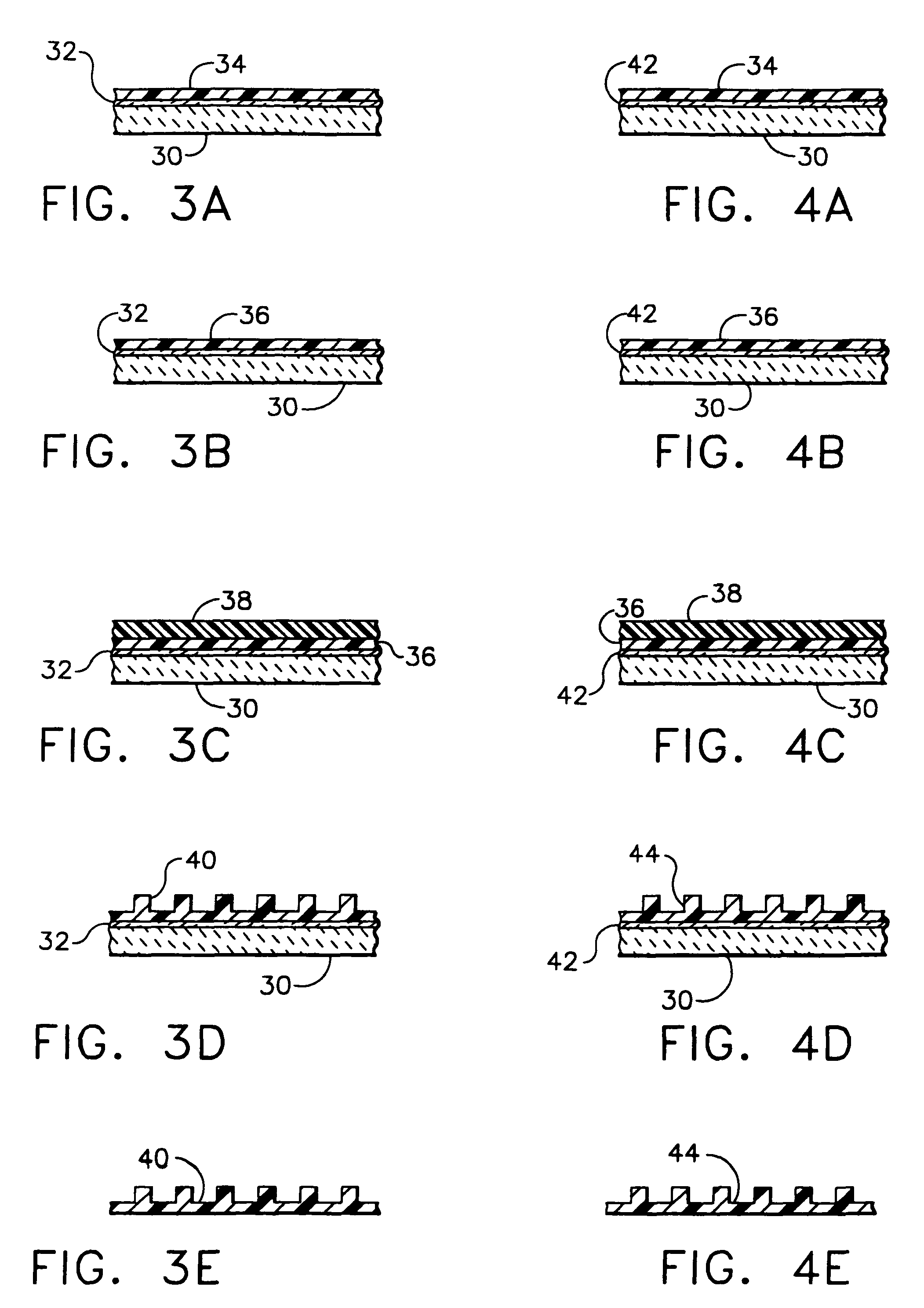
[0048]Using the principles of the present invention, polymeric microneedles can be fabricated by replica molding in which PDMS molds are prepared using a photoresist master. Alternatively, polymeric microneedles can be made by replica molding in which PDMS molds are made utilizing a silicon wafer that is fabricated by deep reactive ion etching or any other etching technique known by those skilled in the art. In both cases, the PDMS material becomes a negative replica which is used as a mold that can be later filled with a prepolymer material that will itself become an array of microneedles. Both solid and hollow microneedles can be made by the techniques of the present invention.
[0049]Although the term “PDMS” is used throughout this patent document in ver...
PUM
| Property | Measurement | Unit |
|---|---|---|
| Size | aaaaa | aaaaa |
| Microstructure | aaaaa | aaaaa |
| Metallic bond | aaaaa | aaaaa |
Abstract
Description
Claims
Application Information


