Differential signal probing system

a signal and probe technology, applied in the field of probe measurement systems, can solve the problems of parasitic interconnection between many parts, noise from external sources such as adjacent conductors, and the inability to test structures,

Inactive Publication Date: 2010-07-27
CASCADE MICROTECH
View PDF1261 Cites 22 Cited by
  • Summary
  • Abstract
  • Description
  • Claims
  • Application Information

AI Technical Summary

Problems solved by technology

As a result of the physical make up of the devices of an integrated circuit, parasitic interconnections exist between many of the parts of the individual devices and between parts of the devices and the wafer on which the devices are fabricated.
Moreover, noise from external sources, such as adjacent conductors, tends to couple, electrically and electromagnetically, in the common mode and cancel in the differential mode.
However, test structures serve no purpose after the dies containing the marketable ICs are singulated and manufacturers of ICs are under continuous cost pressure to maximize the number of marketable ICs that are manufactured on each wafer.

Method used


Image

  • Differential signal probing system
  • Differential signal probing system
  • Differential signal probing system

Examples


Embodiment Construction

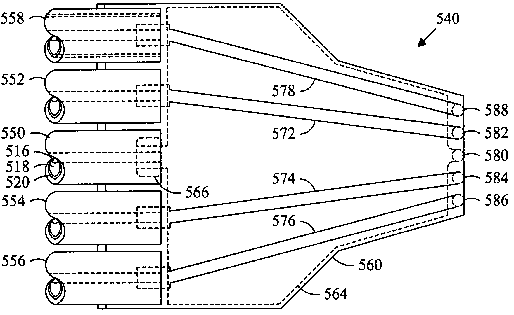
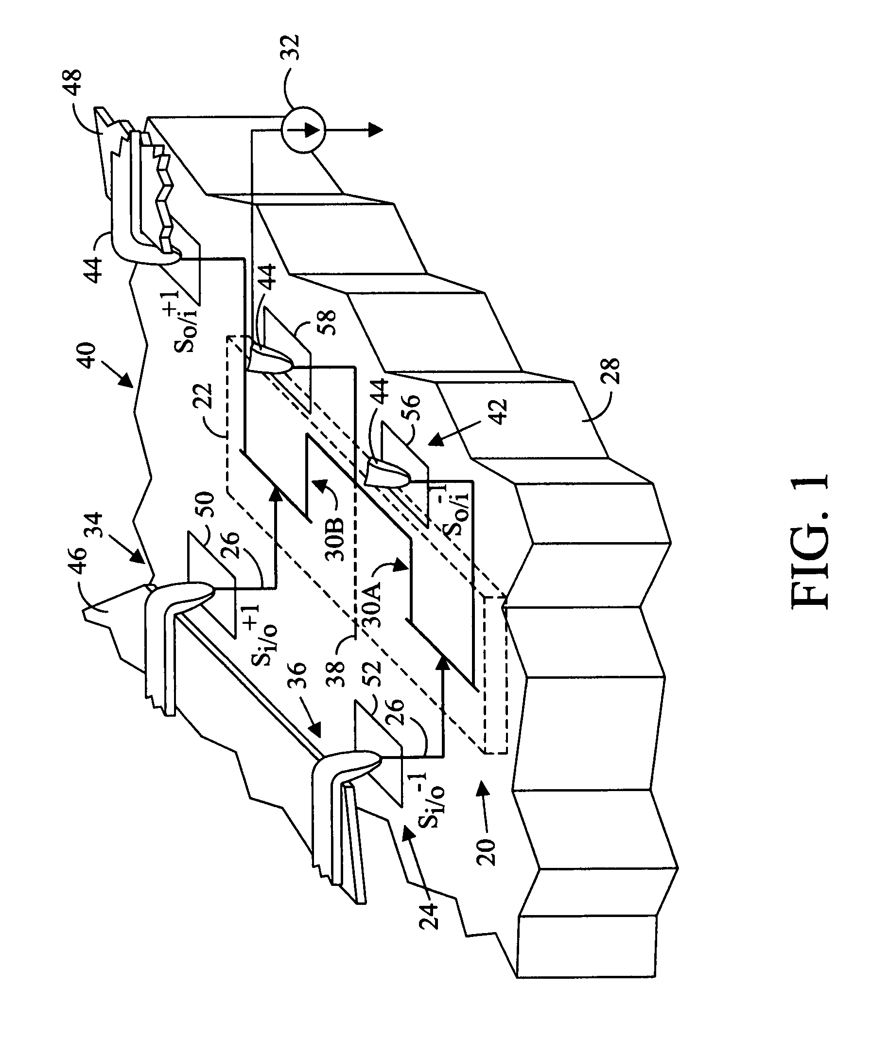
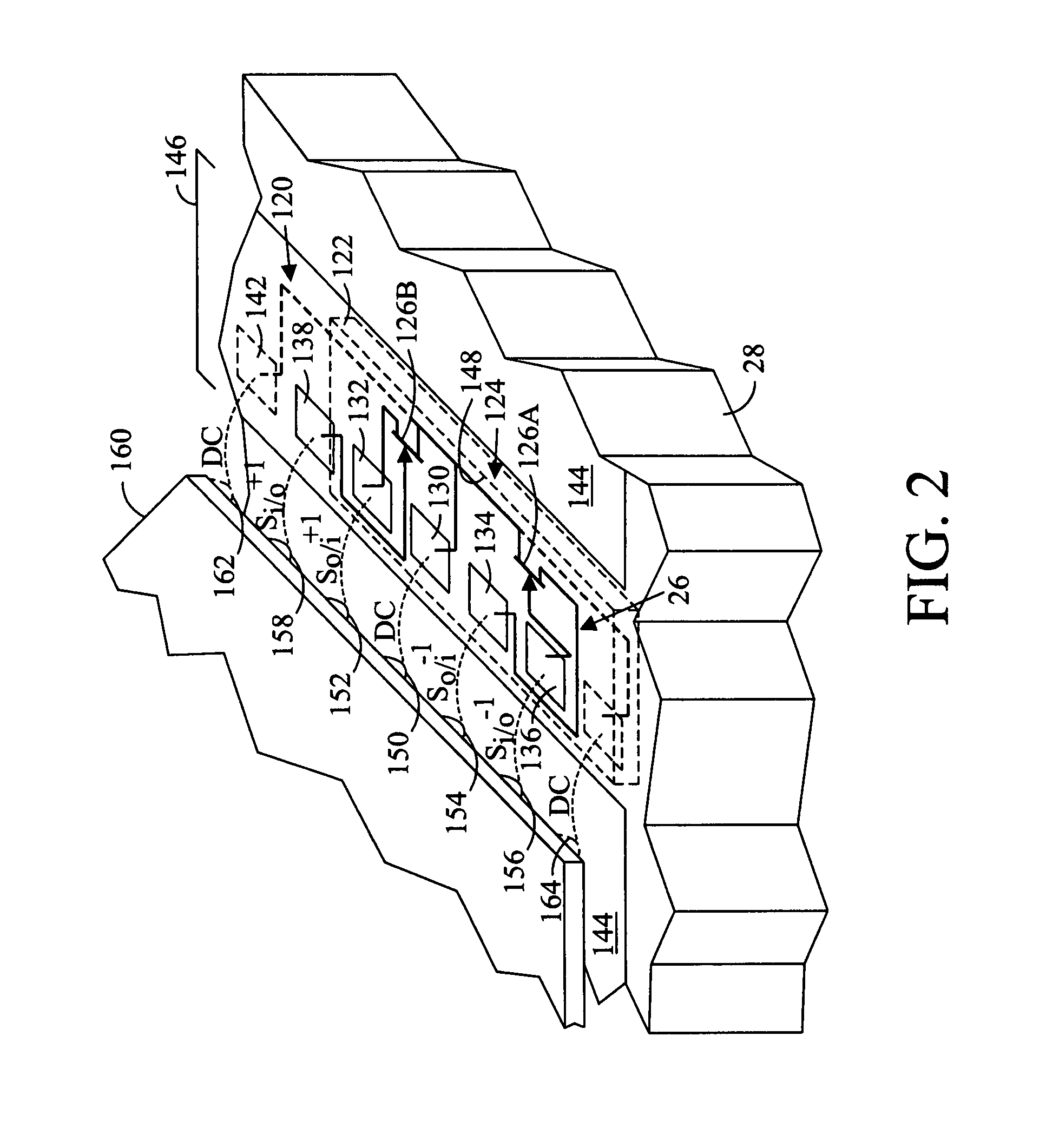
[0029]Circuits utilizing differential signaling are becoming increasingly common for a wide range of higher frequency applications. The benefits of differential signaling or balanced devices include lower power levels, faster state transition for binary devices, good immunity from noise, minimal susceptibility to electromagnetic coupling at higher frequencies, and greater tolerance of poor grounding conditions which are commonly encountered when integrated circuits are operated at high frequencies. The integrity of the process used to manufacture marketable integrated circuits (ICs) is tested by fabricating a plurality of test structures on the wafer using the same process that is used to fabricate the ICs. Characteristics of the marketable ICs are inferred by stimulating the test structure with a test instrument generated signal and capturing the response of the test structure. While test structures are typically simple circuits, the response of similar devices included in the more...


PUM


Abstract

A probe measurement system comprises a probe with a linear array of probe tips enabling a single probe to be used when probing a test structure with a differential signal.

Description

CROSS-REFERENCE TO RELATED APPLICATIONS[0001]This application claims the benefit of U.S. Provisional Application No. 60 / 813,119, filed Jun. 12, 2006 and U.S. Provisional Application No. 60 / 831,477, filed Jul. 17, 2006.BACKGROUND OF THE INVENTION[0002]The present invention relates to probe measurement systems for testing integrated circuits and other microelectronic devices and, more particularly, probe measurement systems utilizing differential signaling for testing microelectronic devices.[0003]Integrated circuits (ICs) are economically attractive because large numbers of often complex circuits, for example microprocessors, can be inexpensively fabricated on the surface of a wafer or substrate. Following fabrication, individual dies, including one or more circuits, are separated or singulated and encased in a package that provides for electrical connections between the exterior of the package and the circuit on the enclosed die. The separation and packaging of a die comprises a sig...

Claims


Application Information

Patent Timeline
Patent Type & Authority Patents(United States)
IPC IPC(8): G01R31/02
CPCG01R1/06772
Inventor STRID, ERICCAMPBELL, RICHARD
Owner CASCADE MICROTECH
Why Eureka
Try Eureka