Semiconductor etching apparatus

a technology of etching apparatus and semiconductors, which is applied in the direction of electrostatic holding devices, basic electric elements, electric devices, etc., can solve the problems of obstructing the process, increasing the temperature of the wafer, and uniform etching, so as to prevent the failure of the etching process

Active Publication Date: 2010-07-27
SAMSUNG ELECTRONICS CO LTD
View PDF10 Cites 5 Cited by
  • Summary
  • Abstract
  • Description
  • Claims
  • Application Information

AI Technical Summary

Benefits of technology

[0015]Therefore, the present invention is directed to provide a semiconductor etching apparatus which prevents polymers from remaining on the upper part of an electro static chuck (ESC) when a wafer is dechucked or transferred, thereby preventing a failure of an etching process due to a wafer chucking failure.
[0016]Embodiments of the present invention provide a semiconductor etching apparatus which prevents polymers from sticking to an electro static chuck (ESC), thereby preventing a failure of an etching process by minimizing a helium leak error due to a wafer chucking failure.

Problems solved by technology

When a layer formed on a wafer is etched, a great amount of heat is inevitably generated, so that a temperature of the wafer increases.
The temperature rise may seriously affect the etching uniformity, thereby obstructing the process.
When the polymers remain on the upper surface of the ESC 10, the wafer cannot be secured against the ESC 10 upon the wafer chucking, thereby causing helium to leak at the backside of the wafer, to cause an error.
When an error is caused, the wafer is not cooled and the temperature suddenly rises.
Then, the impedance of the chamber is changed and the plasma is not stabilized, thereby causing a failure in the etching process.

Method used


Image

  • Semiconductor etching apparatus
  • Semiconductor etching apparatus
  • Semiconductor etching apparatus

Examples


Embodiment Construction

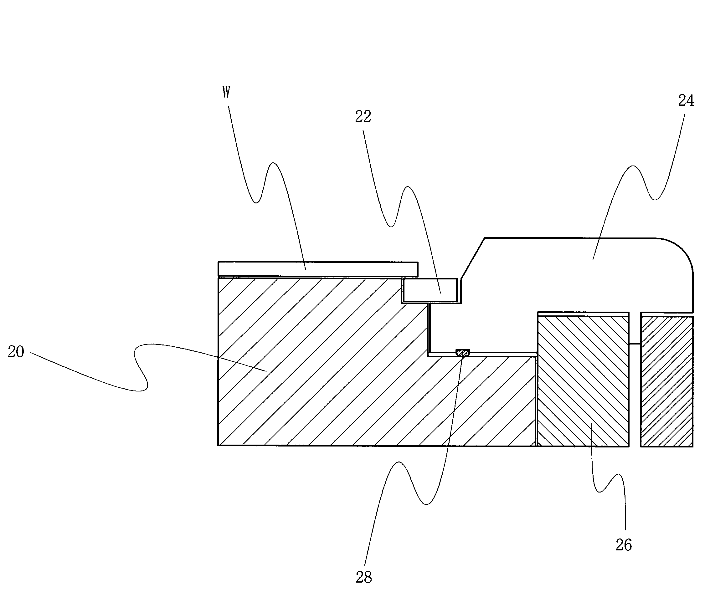
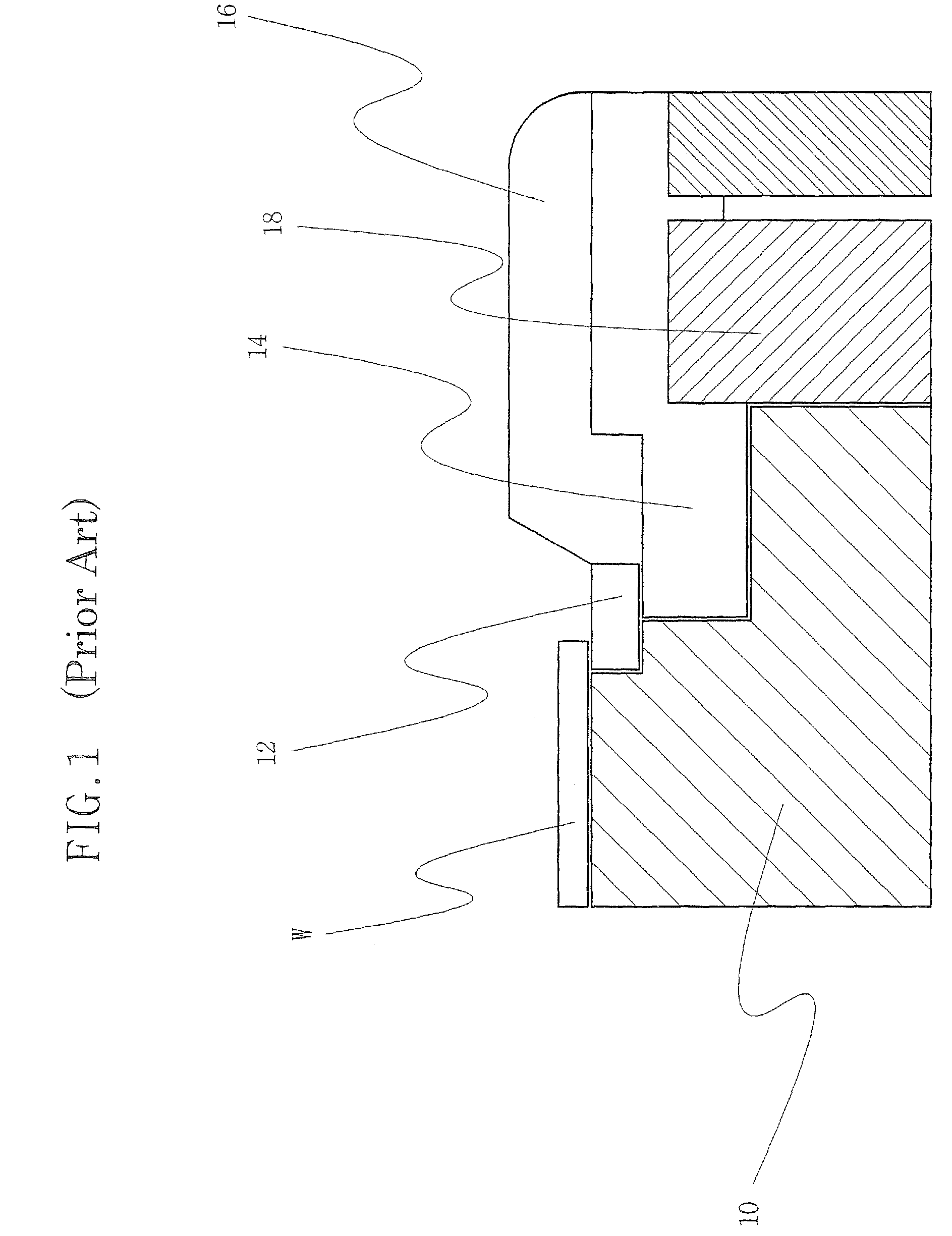
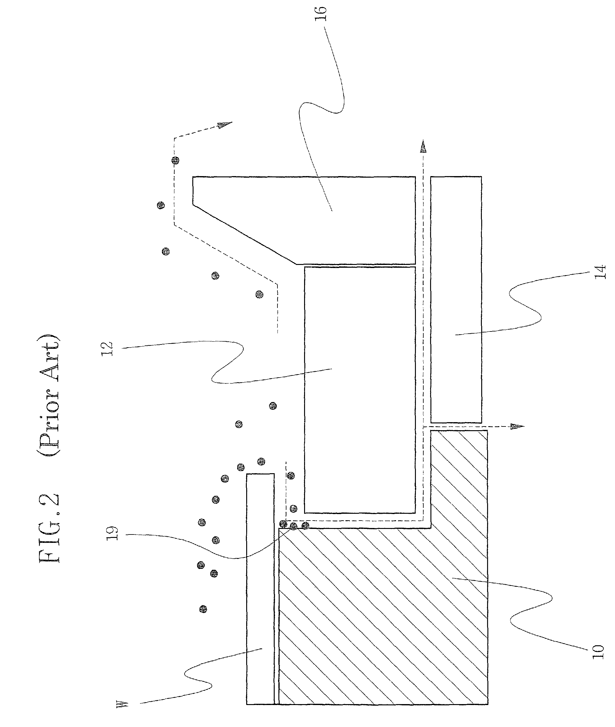
[0027]The invention will be described more fully hereinafter with reference to the accompanying drawings, in which example embodiments of the invention are shown. This invention may, however, be embodied in many different forms and should not be construed as limited to the example embodiments set forth herein. Rather, the disclosed embodiments are provided so that this disclosure will be thorough and complete, and will fully convey the scope of the invention to those skilled in the art. In the drawings, the size and relative sizes of layers and regions may be exaggerated for clarity. Moreover, each embodiment described and illustrated herein includes its complementary conductivity type embodiment as well. Like numbers refer to like elements throughout.

[0028]It will be understood that when an element or layer is referred to as being “on”, “connected to” and / or “coupled to” another element or layer, it can be directly on, connected or coupled to the other element or layer or interveni...


PUM

PropertyMeasurementUnit
sizeaaaaaaaaaa
RF poweraaaaaaaaaa
chucking forceaaaaaaaaaa

Abstract

There is provided a semiconductor etching apparatus which removes particles remaining on the upper surface of an electro static chuck (ESC) during an etching process, thereby preventing a chucking force from decreasing and minimizing a leak of helium. To prevent a failure of the etching process due to a wafer chucking failure, by preventing polymers from falling down on the upper part of the ESC when a wafer is dechucked or transferred, the semiconductor etching apparatus comprises: an ESC selectively holding a wafer to be entered and positioned inside a chamber, and including a lower electrode part to which RF power is applied; parts positioned at a stepped portion of the ESC and respectively surrounding a side of the ESC; and a gas flow blocking part blocking a gas flow in a vacuum path formed between the ESC and the parts.

Description

CROSS-REFERENCE TO RELATED APPLICATION[0001]This application claims the benefit of Korean Patent Application No. 10-2006-0090928, filed Sep. 20, 2006, the disclosure of which is hereby incorporated herein by reference in its entirety.FIELD OF THE INVENTION[0002]The present invention relates to a semiconductor etching apparatus, and more particularly, to a semiconductor etching apparatus structured to remove particles remaining on the upper surface of an electro static chuck (ESC) while an etching process is performed, thereby preventing a chucking force from decreasing and minimizing leakage of helium.BACKGROUND OF THE INVENTION[0003]Generally, a semiconductor device is fabricated by repeatedly performing various fabrication processes on a silicon wafer. Semiconductor fabrication processes include oxidation, masking, photoresist coating, etching, diffusion and layer formation processes with respect to a wafer which is a material of a semiconductor device. Before and after the aforem...

Claims


Application Information

Patent Timeline
Patent Type & Authority Patents(United States)
IPC IPC(8): H02N13/00
CPCH01L21/6831H01L21/68735H01L21/302H01L21/687
Inventor KIM, JIN-MANYANG, YUN-SIKMIN, YOUNG-MINKIM, SANG-HO
Owner SAMSUNG ELECTRONICS CO LTD
Why Eureka
Try Eureka