Method for fabricating wafer level chip scale packages

a technology of chip scale and wafer level, applied in the direction of semiconductor devices, semiconductor/solid-state device details, electrical apparatus, etc., to achieve the effect of avoiding wafer warpage issues

Active Publication Date: 2010-08-17
POWERTECH TECHNOLOGY
View PDF22 Cites 33 Cited by
  • Summary
  • Abstract
  • Description
  • Claims
  • Application Information

AI Technical Summary

Benefits of technology

[0013]4. Through the formation of the underfill gap between the wafer and the protection film on the mold plate by the lamination step and the wafer singulation to chips performed before encapsulation, the encapsulant will completely encapsulate the chips during encapsulation to avoid wafer warpage issues caused by the stresses due to curing of the encapsulant.

Problems solved by technology

Secondly, the wafer is laminated to a mold plate with a protection film placed on the mold plate so that the bumps are partially embedded into the protection film and an underfill gap is formed between the wafer and the protection film.

Method used


Image

  • Method for fabricating wafer level chip scale packages
  • Method for fabricating wafer level chip scale packages
  • Method for fabricating wafer level chip scale packages

Examples


Embodiment Construction

[0018]With reference to the attached drawings, the present invention is described by means of the embodiment(s) below where the attached drawings are simplified for illustration purposes only to illustrate the structures or methods of the present invention by describing the relationships between the components and assembly in the present invention. Therefore, the components shown in the figures are not expressed with the actual numbers, actual shapes, actual dimensions, nor with the actual ratio. Some of the dimensions or dimension ratios have been enlarged or simplified to provide a better illustration. The actual numbers, actual shapes, or actual dimension ratios can be selectively designed and disposed and the detail component layouts may be more complicated.

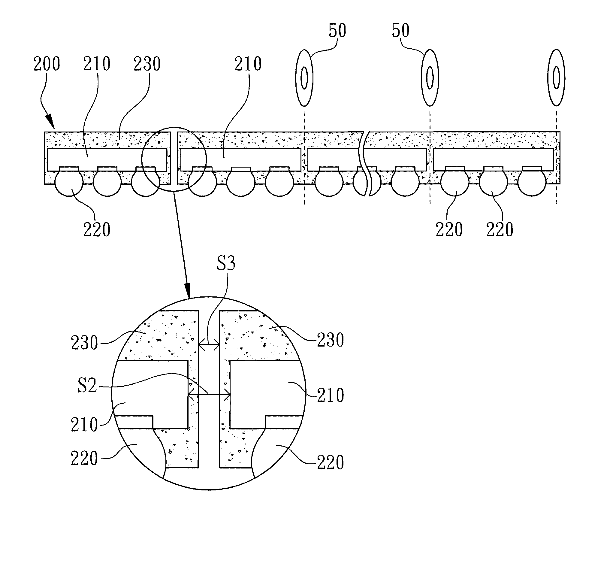
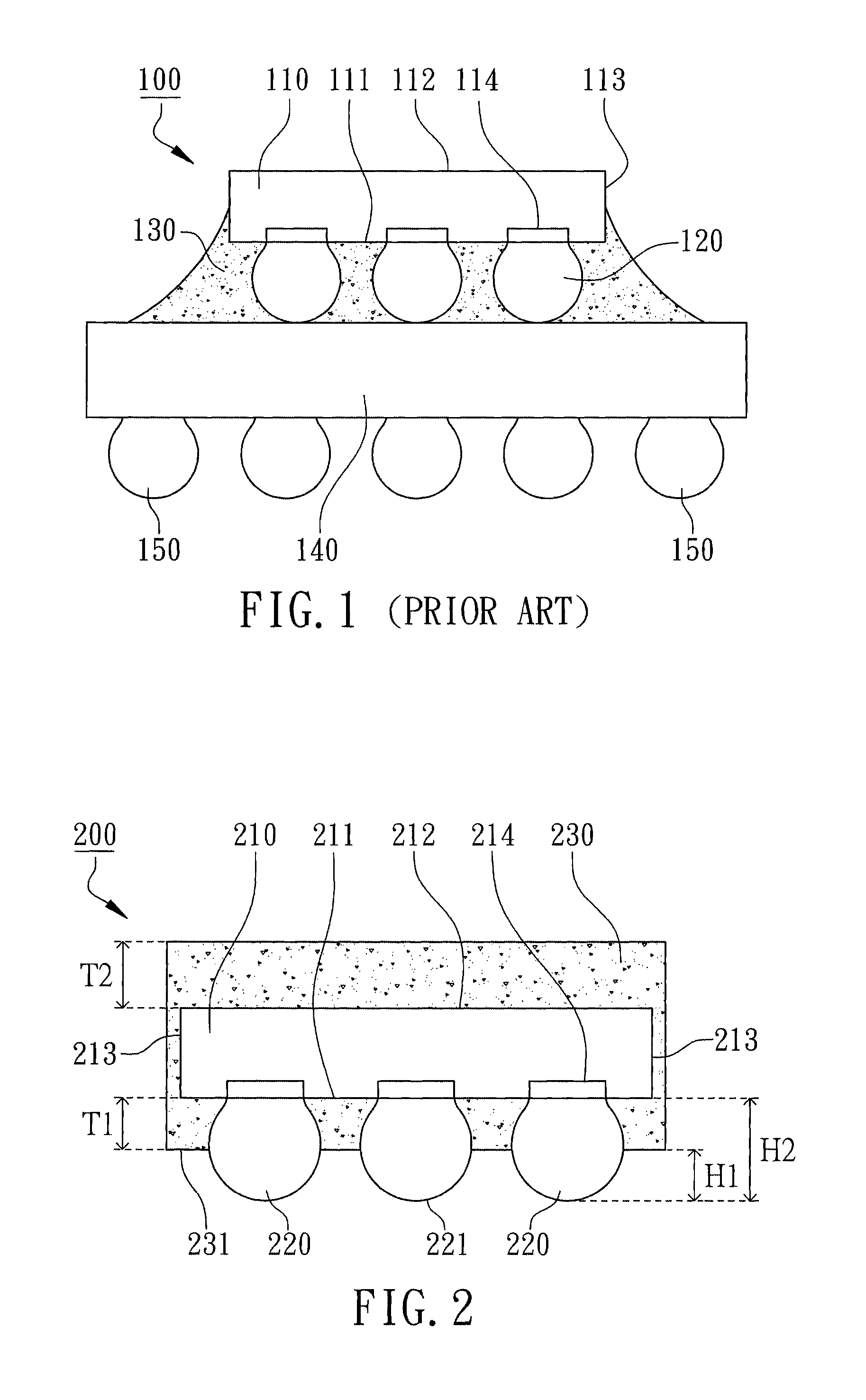
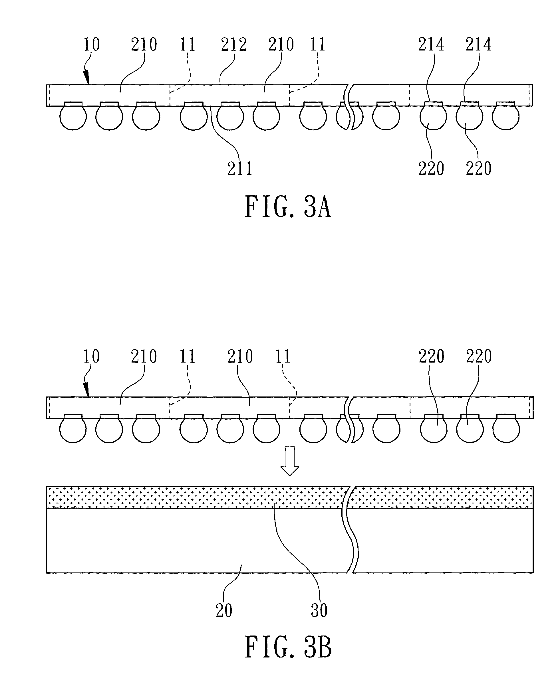
[0019]According to the first embodiment of the present invention, a wafer level chip scale package is illustrated in FIG. 2 for a cross-sectional view. The wafer level chip scale package 200 primarily comprises a chip 210, a ...


PUM


Abstract

A method for fabricating a plurality of wafer level chip scale packages is revealed. A bumped wafer is laminated with a mold plate with a protection film placed thereon to partially embed the bumps of the wafer into the protection film and to form an underfill gap between the wafer and the protection film. By a first sawing step, the wafer fixed by the protection film is singulated into a plurality of chips having sides between the active surface and the back surface and also a filling gap is formed between the sides. Then, an encapsulant is formed on the protection film where the encapsulant fills the underfill gap through the filling gap to completely encapsulate the chips and the non-embedded portions of the bumps. By separating the encapsulant from the protection film and a second sawing step, the mold plate and the protection film are removed, and the encapsulant is singulated into a plurality of individual wafer level chip scale packages.

Description

FIELD OF THE INVENTION[0001]The present invention relates to semiconductor devices, and more particularly to methods for fabricating a plurality of wafer level chip scale packages (WLCSP).BACKGROUND OF THE INVENTION[0002]In conventional semiconductor packages, chips are disposed on larger substrates where the internal electrical connections between chips and substrates can be divided into two major methodologies, flip-chip bonding and wire bonding. For flip-chip bonding, bumps are pre-disposed on chips then flipped and joined the bumped chips on substrates to achieve electrical connections through bumps. Normally, semiconductor packages will be surface-mounted on external printed circuit boards as electronic components, and therefore, substrates are served as external electrical interposers. Moreover, since the dimensions of substrates are larger than the ones of chips, therefore, semiconductor packages can not meet the specifications of wafer level chip scale packages.[0003]As show...

Claims


Application Information

Patent Timeline
Patent Type & Authority Patents(United States)
IPC IPC(8): H01L21/00
CPCH01L23/3114H01L21/561H01L21/568H01L21/6836H01L2924/01013H01L2924/01029H01L2924/01046H01L2924/01047H01L2924/01074H01L2924/01078H01L2924/01079H01L2924/01082H01L2924/15311H01L2924/01033H01L24/11H01L24/12H01L24/94H01L2221/68327H01L2221/6834H01L2221/68381H01L2224/05124H01L2224/05147H01L2224/05644H01L2224/05647H01L2224/05666H01L2224/05684H01L2224/1132H01L2224/11462H01L2224/13022H01L2224/13111H01L2224/13124H01L2224/13139H01L2224/13144H01L2224/13147H01L2224/13155H01L2224/13164H01L2224/13169H01L2224/13562H01L2224/1357H01L2224/136H01L2224/94H01L2224/0401H01L2924/00014H01L2224/03H01L2924/014
Inventor FAN, WEN-JENG
Owner POWERTECH TECHNOLOGY
Why Eureka
Try Eureka