Bipolar transistor with raised base connection region and process for the production thereof

a bipolar transistor and raised base technology, applied in transistors, electrical devices, semiconductor devices, etc., can solve the problems of large width of the boundary between the emitter and the outer base layer relative to the inner base layer, and in part even at its greatest width, so as to reduce the base resistance, reduce the effect of doping and low emitter resistan

Active Publication Date: 2010-08-17
IHP GMBH INNOVATIONS FOR HIGH PERFORMANCE MICROELECTRONICS LEIBNIZ INST FUR INNOVATIVE
View PDF11 Cites 9 Cited by
  • Summary
  • Abstract
  • Description
  • Claims
  • Application Information

AI Technical Summary

Benefits of technology

[0013]In comparison with the known state of the art the technical object involved is that of providing a bipolar transistor having a low base resistance, which can be produced at a low level of complication and expenditure and in which the base and the emitter are improved in terms of good high frequency suitability for use of the bipolar transistor.

Problems solved by technology

A disadvantage of the previously known structures described is accordingly in particular that the insulation between the emitter and the outer base layer at the boundary relative to the inner base layer is of a large width and in part is even at its greatest width.

Method used


Image

  • Bipolar transistor with raised base connection region and process for the production thereof
  • Bipolar transistor with raised base connection region and process for the production thereof
  • Bipolar transistor with raised base connection region and process for the production thereof

Examples


example 1

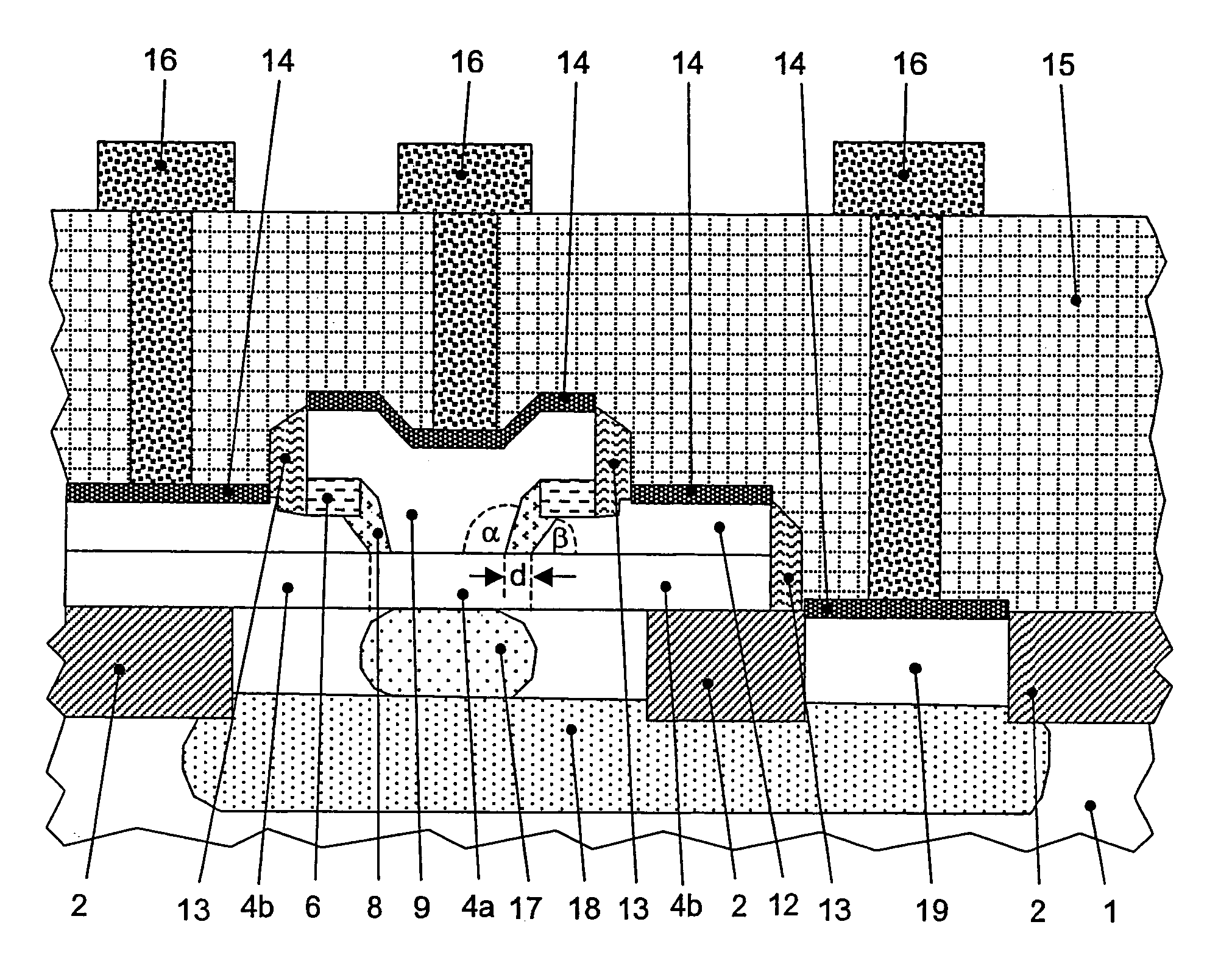
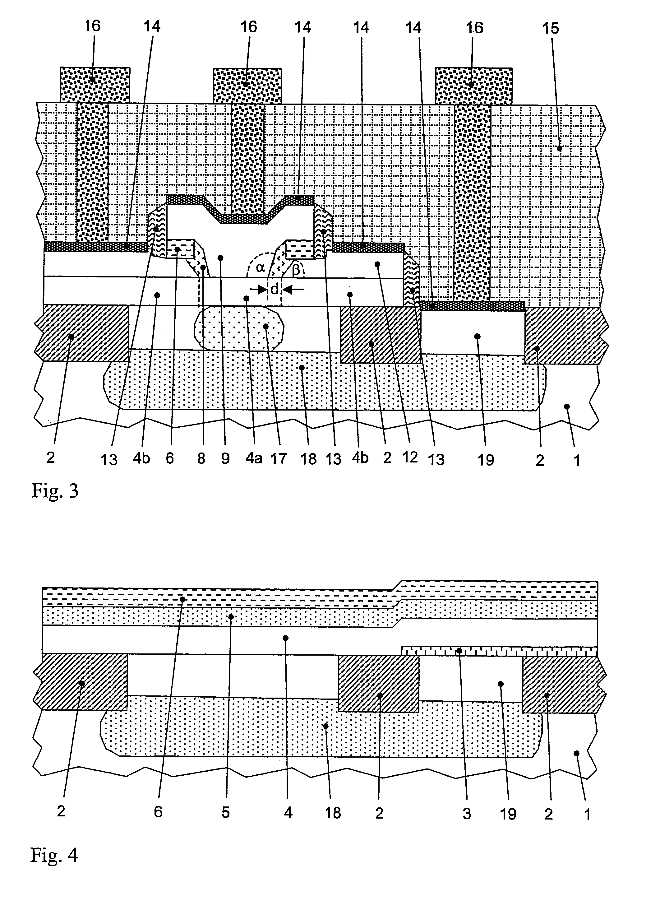
[0078]FIG. 3 is a cross-sectional view showing the structure of an embodiment of the bipolar transistor of the invention. In this example an npn-transistor with an epitaxial base is produced on a high-ohmic, p-conducting Si substrate 1. The essential features of the described arrangement can also be applied to other substrate dopings and pnp-transistors.

[0079]The npn-transistor includes an n-conducting emitter 9, a p-conducting base 4 and an n-conducting collector 17. The collector is brought into contact by way of an n-conducting region 18 and an n-conducting collector connection region 19. Arranged above the collector region is a first epitaxial base layer 4 which contains a p-doping. In particular the epitaxial base layer can include an SiGe layer. For example the epitaxial base layer can include a layer sequence Si / SiGe / Si. In addition the epitaxial base layer can be doped with carbon. The epitaxial base layer can be particularly advantageously produced by differential epitaxy. ...

example 2

[0091]A first process for the production of a bipolar transistor with a raised base connection region will now be described with reference to FIGS. 4 through 9. In the following Figures the same structural elements are denoted by the same references.

[0092]In particular the process according to the invention permits the production of high-speed bipolar transistors in integrated bipolar and BiCMOS procedures.

[0093]The embodiment involves a process for the production of npn-bipolar transistors on a p-conducting substrate 1. Active regions and insulating regions 2 are structured on the substrate 1. By way of example n-conducting regions 18, 19 were produced in the region of the collector of the transistor by masked ion implantation.

[0094]n-Conducting and p-conducting wells are produced in the CMOS regions and gates of polysilicon are structured and provided with lateral spacers.

[0095]An auxiliary layer 3 is deposited on the Si wafers structured as described. That auxiliary layer can be ...

example 3

[0110]A second process for the production of a bipolar transistor with a raised base connection region differs from the process described in Example 2 essentially in that the raised base connection region is not deposited in self-adjusted relationship with the emitter window. That process will now be described with reference to FIGS. 10 and 11.

[0111]Up to deposit of the base layer 4 the process is identical to the process described in Example 2. An insulating layer 20 is then deposited on the base layer 4. That insulating layer preferably comprises silicon dioxide and is preferably of a thickness of between 40 nm and 150 nm.

[0112]An emitter window is structured in the insulating layer 20 by way of a lacquer mask. The emitter 9 is deposited in a further step. The emitter preferably comprises silicon which is provided in situ with an n+-doping. The emitter can be monocrystalline or polycrystalline in the region of the emitter window. An insulating layer 21 which preferably comprises s...


PUM


Abstract

A bipolar transistor has a base with an epitaxial base layer and a raised base connection region which in a lateral direction in parallel relationship with the substrate surface encloses the emitter which is surrounded by a spacer of insulating material. The epitaxial base layer is raised in a heightwise direction perpendicularly to the substrate surface. An emitter of a T-shaped cross-sectional profile is separated laterally from the outer base portion by a spacer of insulating material. Its vertical bar of the T-shape adjoins with its lower end the inner base portion. The lateral extent of the spacer increases from its interface with respect to the base layer with increasing height above the base layer, wherein a first interface formed by the emitter and the spacer meets a second interface formed by the emitter and the inner base portion at a first angle which is either a right angle or an obtuse angle, and a third interface formed by the spacer and the outer base portion meets the second interface at a second obtuse angle which is larger than the first angle.

Description

CROSS REFERENCE TO RELATED APPLICATIONS[0001]This application is for entry into the U.S. national phase under §371 for International Application No. PCT / EP2004 / 013954 having an international filing date of 3 Dec. 2004, and from which priority is claimed under all applicable sections of Title 35 of the United States Code including, but not limited to, Sections 120, 363 and 365(c), and which in turn claims priority under 35 USC §119 to German Patent Application No. DE 103 58 046.8 filed on 5 Dec. 2003.BACKGROUND OF THE INVENTION[0002]1. Technical Field[0003]The invention relates to a bipolar transistor with raised base connection region and a process for the production thereof.[0004]2. Discussion of Related Art[0005]Bipolar transistors are used in many different ways in integrated analog and digital electronic circuits. In particular, bipolar transistors are used for high-speed uses because of their short switching times. It was possible to considerably increase the operational effici...

Claims


Application Information

Patent Timeline
Patent Type & Authority Patents(United States)
IPC IPC(8): H01L31/072H01L21/331H01L29/06H01L29/10H01L29/732H01L29/737
CPCH01L29/0649H01L29/66242H01L29/66287H01L29/732H01L29/7378H01L29/1004
Inventor RÜCKER, HOLGERHEINEMANN, BERND
Owner IHP GMBH INNOVATIONS FOR HIGH PERFORMANCE MICROELECTRONICS LEIBNIZ INST FUR INNOVATIVE
Why Eureka
Try Eureka