Transistor structure with minimized parasitics and method of fabricating the same

a transistor and structure technology, applied in the field of bipolar transistors, can solve the problems of reducing the overall performance of the device, disadvantageously affecting the cut off frequency (fsub>t/sub>) and maximum oscillation frequency, and increasing the parasitic effect of the device, so as to achieve the effect of reducing the parasitic effect and high performan

Inactive Publication Date: 2006-07-11
GLOBALFOUNDRIES INC
View PDF4 Cites 9 Cited by
  • Summary
  • Abstract
  • Description
  • Claims
  • Application Information

AI Technical Summary

Benefits of technology

[0013]One object of the present invention is to provide a high performance bipolar transistor having reduced parasitic effects, thereby providing an optimized cut-off frequency and the maximum oscillation frequency.
[0014]Another object of the present invention is to provide a method for forming a new NPN transistor device structure that concurrently minimizes parasitic effects such as the base resistance (Rb), collector resistance (Rc), emitter resistance (Re), emitter-base capacitance (Ceb), collector-emitter capacitance (Cce), collector-base capacitance (Ccb), and collector-substrate capacitance (Ccs).
[0015]These and other objects and advantages are achieved in the present invention by forming a bipolar transistor in which the emitter region is recessed to reduce the extrinsic portion of the emitter and to reduce the width of the base / emitter spacer. Recessing the emitter below the horizontal surfaces of the extrinsic base regions substantially reduces the parasitic emitter base capacitance (Ceb) and emitter series resistance (Re). Broadly, the inventive bipolar transistor comprises:
[0029]Another aspect of the present invention is a bipolar transistor comprising silicided extrinsic base regions, where the silicided region is positioned on substantially the entire horizontal surface of the extrinsic base region and abuts the emitter base isolation spacer. Siliciding the entire horizontal surface of the extrinsic base regions substantially reduces the parasitic base resistance (Rb) of the device. Broadly, the inventive bipolar transistor comprises:
[0044]Another aspect of the present invention is a bipolar transistor, which minimizes the collector-base capacitance (Ccb). Specifically, the intrinsic component of the collector-base capacitance (Ccb,int) is reduced by reducing the area of the pedestal implant region 27 and the extrinsic component of the collector-base capacitance (Ccb,ext) may be reduced by reducing the length of a base contact window (BX) such that the area of the base contact window (BX) is smaller than the active area (RX) of the device. Broadly, the inventive bipolar transistor structure comprises:
[0056]Additionally, the collector substrate capacitance (Ccs) may be reduced by using a low dielectric material as fill for the deep trench.

Problems solved by technology

The above modifications, which may increase the cut off frequency (fT), may also increase parasitic effects within the device, disadvantageously effecting the maximum oscillation frequency (fmax).
In addition to the above parasitics, the parasitic elements of the emitter-base capacitance (Ceb) and the emitter resistance (Re) may also disadvantageously affect the cut off frequency (fT) and maximum oscillation frequency (fmax), particularly at low current.
Currently, in NPN devices, one or more parasitic elements could be reduced by existing production means but disadvantageously at the expense of other increased parasitic effects resulting in a decreased performance device overall.
U.S. Patent Application No. 2003 / 0057458 provides one prior NPN transistor having a shallow junction raised extrinsic base, where increasing the distance between the collector pedestal and the extrinsic base reduces the collector-base capacitance (Ccb), but disadvantageously tends to increase the parasitic base resistance (Rb).

Method used


Image

  • Transistor structure with minimized parasitics and method of fabricating the same
  • Transistor structure with minimized parasitics and method of fabricating the same
  • Transistor structure with minimized parasitics and method of fabricating the same

Examples


Embodiment Construction

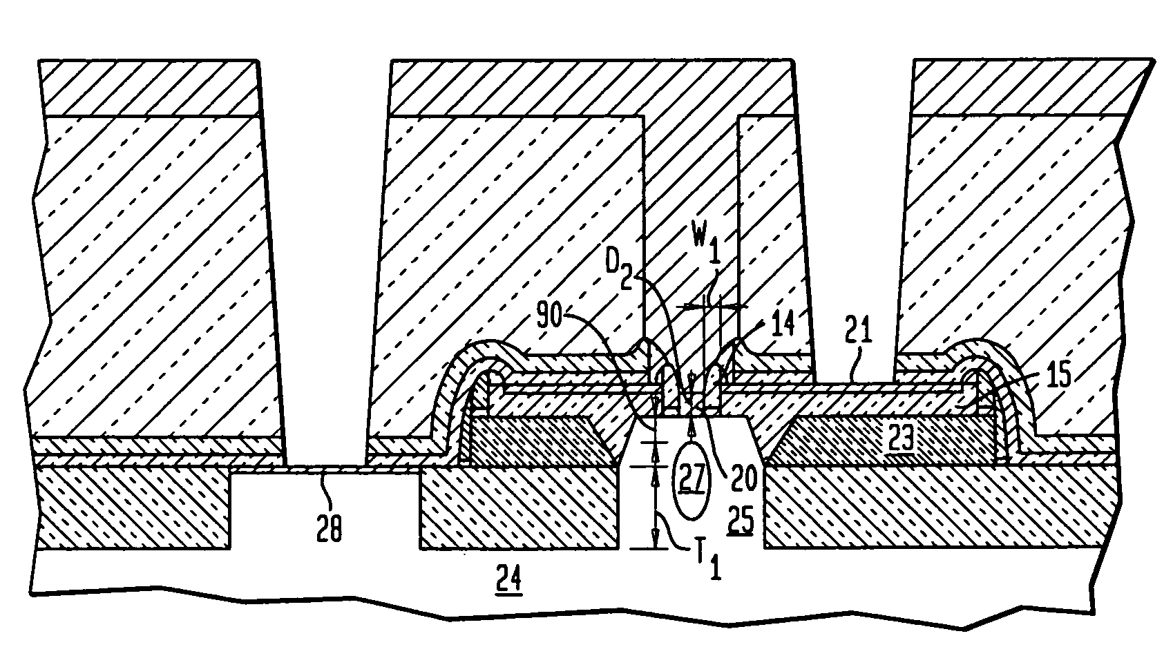
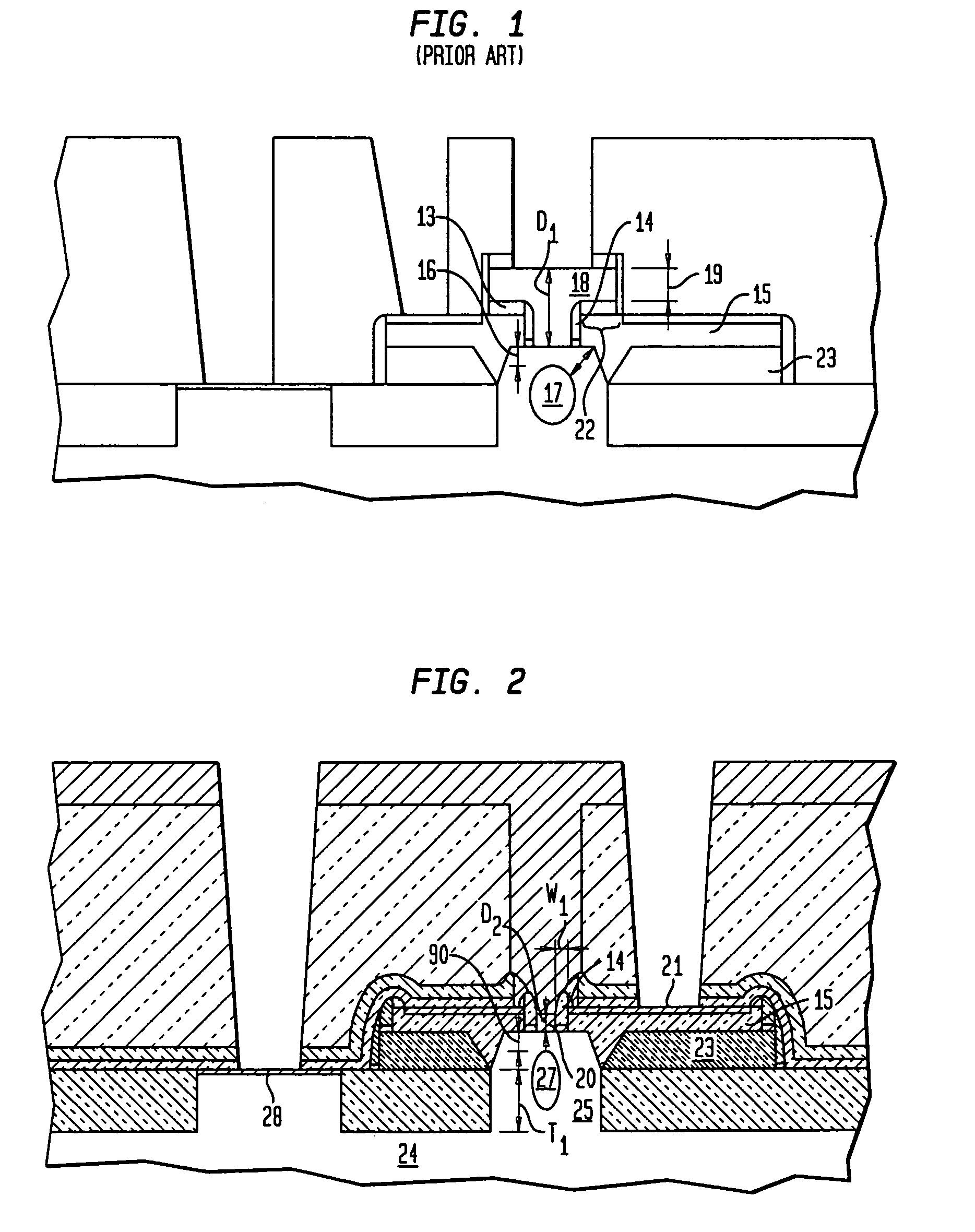
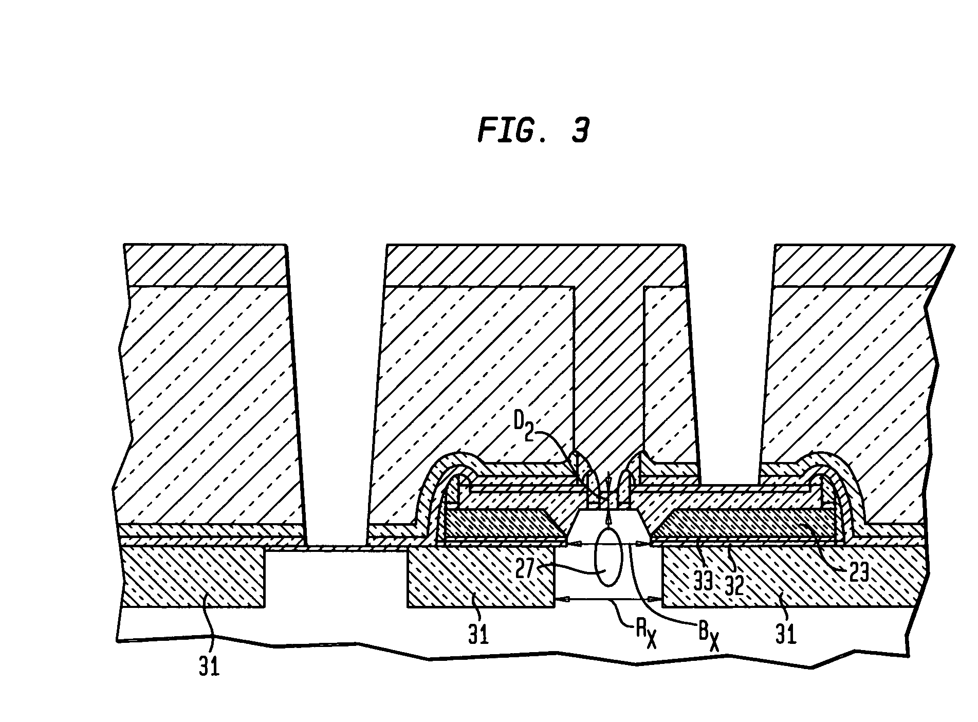
[0062]The present invention directed to a bipolar transistor having improved maximum oscillation frequency (fmax), and a method of fabricating a bipolar transistor having improved maximum oscillation frequency (fmax), will now be described in greater detail by referring to the drawings that accompany the present application. For simplicity, a single bipolar device region is shown in the drawings. It is understood that other bipolar device regions as well as digital logic circuitry (not shown) may be formed adjacent to the bipolar device region depicted in the drawings. In the accompanying drawings, like and or corresponding elements are referred to by like reference numbers.

[0063]Referring to FIG. 2 illustrating one embodiment of the present invention, a bipolar transistor is provided having a recessed emitter 20 and optimized emitter to base spacers 14 (herein after emitter / base spacers). The recessed emitter 20 reduces the emitter resistance (Re) and the emitter-base capacitance (...


PUM


Abstract

A transistor having minimized parasitics is provided including an emitter having a recessed extrinsic emitter portion atop an intrinsic emitter portion; a base including an intrinsic base portion in electrical contact with the intrinsic emitter portion and an extrinsic base portion in electrical contact with the intrinsic base portion and electrically isolated from the recessed extrinsic emitter portion by a set of emitter / base spacers; and a collector in electrical contact with the intrinsic base portion. The transistor may further include extrinsic base having top surfaces entirely silicided to the emitter / base spacer. Additionally, the transistor may include a base window opening within the transistor's active area. Methods of forming the above-described transistor are also provided.

Description

CROSS REFERENCE TO RELATED APPLICATIONS[0001]This application relates to commonly owned, co-pending published U.S. Patent Application No. 2003 / 0057458 entitled BIPOLAR DEVICE HAVING SHALLOW JUNCTION RAISED EXTRINSIC BASE AND METHOD FOR MAKING THE SAME, filed Sep. 25, 2001, the whole contents and subject matter of which is incorporated by reference as if fully set forth herein.FIELD OF THE INVENTION[0002]The present invention relates to bipolar transistors (BJT), and more particularly to a BJT structure and method of fabricating the same that exhibits less detrimental parasitic effects and improved performance.BACKGROUND OF THE INVENTION[0003]Electrically, bipolar transistors can be thought of as two diodes back to back. The current flows from the emitter region through the base into the collector. When there is no current to the base, the transistor is turned off. When it is on, the current flows. It only takes a small current to turn the base on enough to allow current flow through...

Claims


Application Information

Patent Timeline
Patent Type & Authority Patents(United States)
IPC IPC(8): H01L29/737H01L21/331H01L29/08H01L29/423H01L29/72H01L29/73H01L29/732
CPCH01L29/0804H01L29/0821H01L29/42308H01L29/7378H01L29/66287H01L29/732H01L29/66242
Inventor GREENBERG, DAVID R.JENG, SHWU-JEN
Owner GLOBALFOUNDRIES INC
Why Eureka
Try Eureka