Semiconductor socket with direct selective metalization

a technology of semiconductor sockets and semiconductors, applied in the manufacture of contact parts, metallic pattern materials, basic electric elements, etc., can solve the problems of mechanical and electrical limitations of traditional devices, limiting the space available for locating springs or contact parts that can deflect, and reducing the surface area available for placing contacts. , to achieve the effect of improving electrical performance or internal function and intelligence, improving the reliability of solder joints, and enhancing substrates

Active Publication Date: 2015-10-01
HSIO TECH
View PDF7 Cites 17 Cited by
  • Summary
  • Abstract
  • Description
  • Claims
  • Application Information

AI Technical Summary

Benefits of technology

[0021]The substrate containing the contact members may be inverted to expose the proximal ends of the contact members that will electrically couple with the printed circuit board. This surface of the substrate and the array of exposed proximal ends of the contact members may be processed to achieve contact retention, to add mechanical features to improve the reliability of the solder joint to the printed circuit board, and to provide a platform to add passive and active circuit features to improve electrical performance or internal function and intelligence.
[0022]Once the substrate is loaded with contact members, the substrate can be processed as a printed circuit board or semiconductor package to add functions and electrical enhancements not found in traditional connectors. In one embodiment, electrical devices and conductive traces are plated onto the substrate using, for example, electro-less plating, inkjet printing technology, aerosol printing technology, or other printing technology. The ability to enhance the substrate such that it mimics aspects of the IC package and the printed circuit board allows for reductions in complexity for the IC package and the printed circuit board while improving the overall performance of the semiconductor socket.
[0023]The present process permits the fabrication of functional structures, such as conductive paths and electrical devices, without the use of masks or resists. Features down to about 10 microns can be directly written in a wide variety of functional inks, including metals, ceramics, polymers and adhesives, on virtually any substrate-silicon, glass, polymers, metals and ceramics. The substrates can be planar and non-planar surfaces. The process is typically followed by a thermal treatment, such as in a furnace or with a laser, to achieve dense functionalized structures.
[0024]The use of processes disclosed herein permits the material set in a given layer to vary. Traditional printed circuit board and circuit fabrication methods take sheets of material and stack them up, laminate, and / or drill. The materials in each layer are limited to the materials in a particular sheet. Imaging the liquid dielectric permit a wide variety of materials to be applied on a layer with a registration relative to the features of the previous layer. Selective addition of conductive, non-conductive, or semi-conductive materials at precise locations to create a desired effect may have advantages in tuning impedance or adding electrical function on a given layer. Tuning performance on a layer by layer basis relative to the previous layer can greatly enhance electrical performance.
[0025]The present method and apparatus can permit dramatic simplification of the contact members and the substrate of the socket housing. The preferably featureless contact members reduce parasitic effects of additional metal features normally present for contact member retention. The present method and apparatus can be compatible with existing high volume manufacturing techniques. Adding functions to the socket housing permits reductions in the cost and complexity of the IC package and / or the printed circuit board.
[0026]In another embodiment, mechanical decoupling features are added to the contact member retention structure. The semiconductor socket can be configured to electrically and mechanically couple to contact pads on the printed circuit board, thereby reducing cost and eliminating at least one reflow cycle that can warp or damage the substrate.

Problems solved by technology

As systems advance to next generation architectures, these traditional devices have reached mechanical and electrical limitations that mandate alternate approaches.
As the terminal pitch reduces, however, the surface area available to place a contact is also reduced, which limits the space available to locate a spring or a contact member that can deflect without touching a neighbor.
Thinner walls increase the difficulty of molding as well as the latent stress in the molded housing that can cause warping due to heat applied during solder reflow.
Long contact members, however, tend to reduce the electrical performance of the connection by creating a parasitic effect that impacts the signal as it travels through the contact.
Also, the small space between contact members can cause distortion as a nearby contact member influences a neighboring contact member, which is known as cross talk. the mechanical compliance requirements of today's needs, but they have reached an electrical performance limit.
Next generation systems will operate above 5 GHz and beyond and the existing interconnects will not achieve acceptable performance levels without significant revision.

Method used


Image

  • Semiconductor socket with direct selective metalization
  • Semiconductor socket with direct selective metalization
  • Semiconductor socket with direct selective metalization

Examples


Embodiment Construction

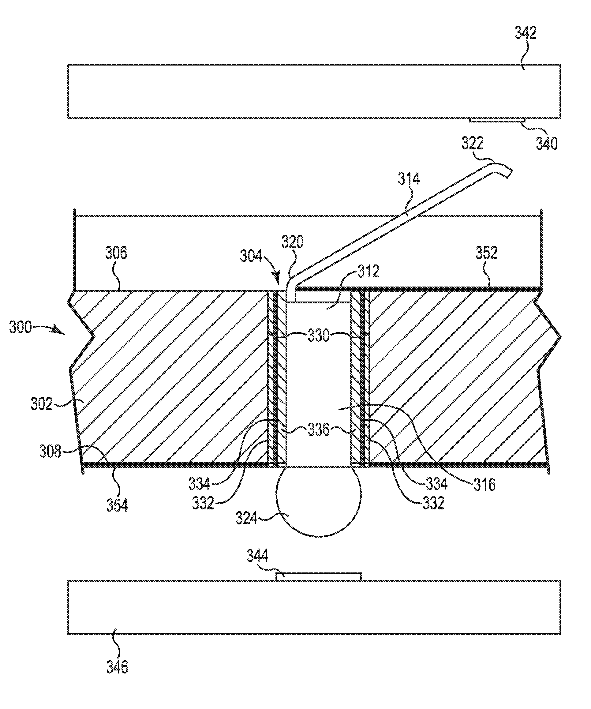
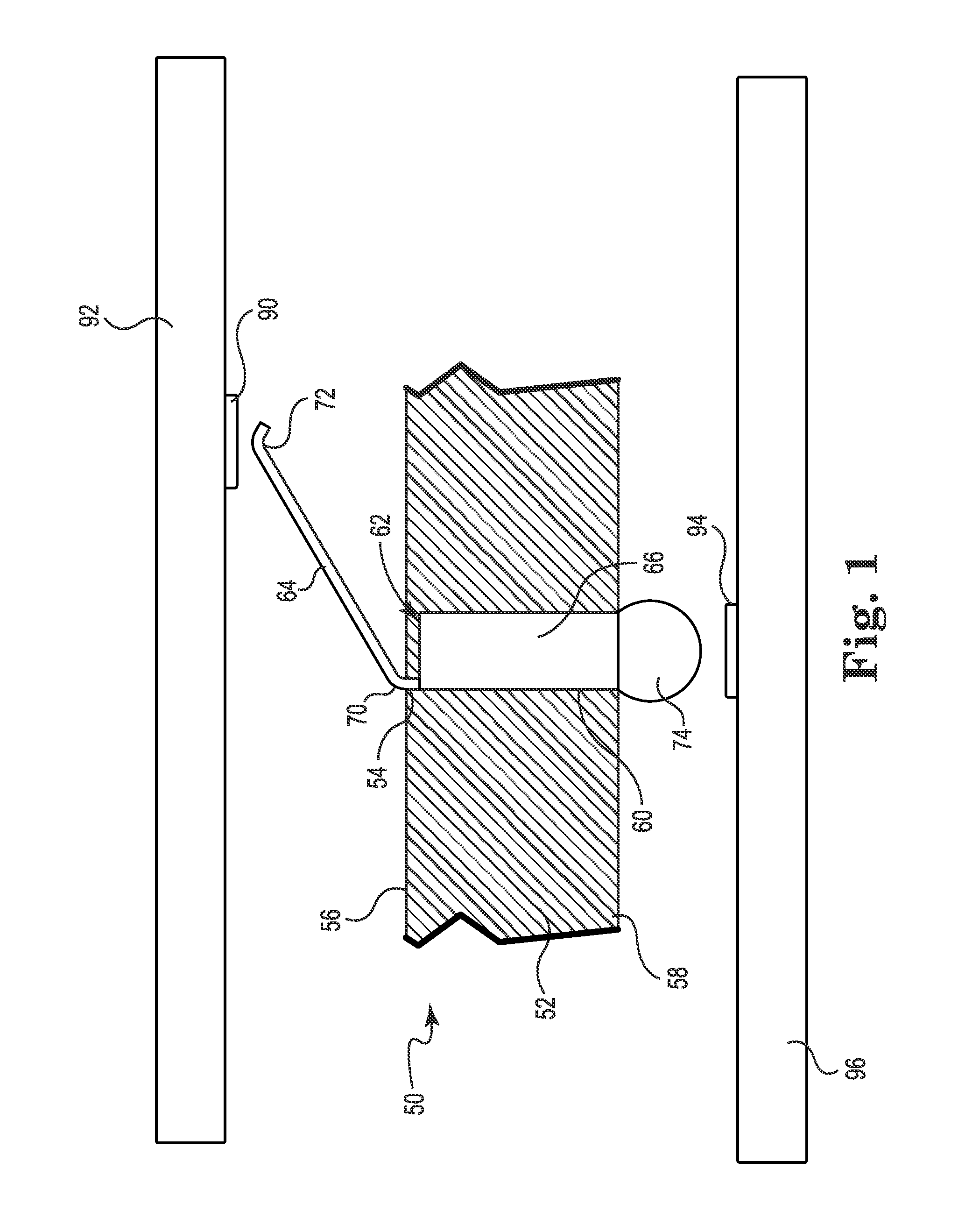
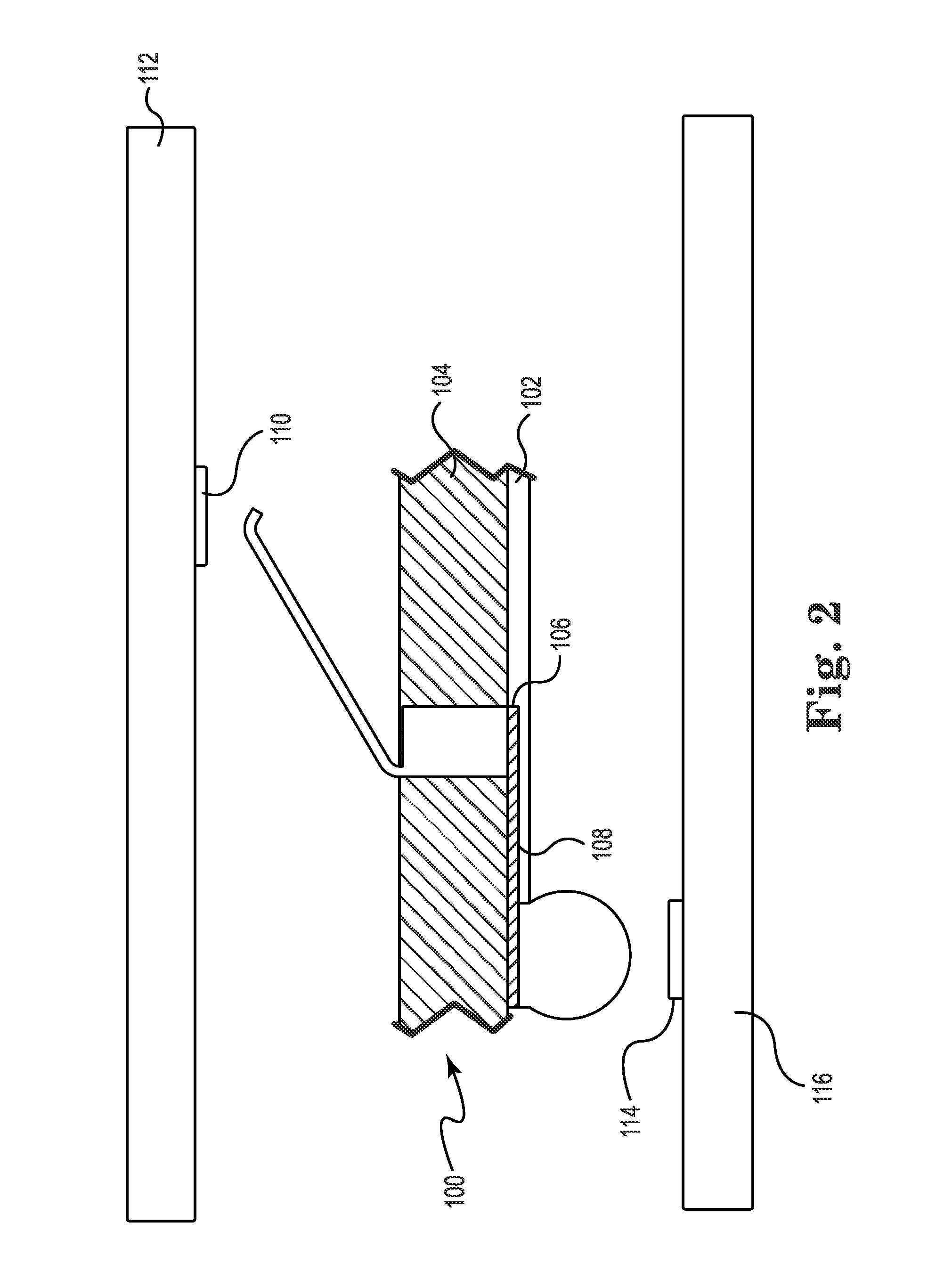
[0040]A semiconductor socket in accordance with the present disclosure permits fine contact-to-contact spacing (pitch) on the order of less than 1.0 millimeter (1×10⁻³ meter), and more preferably a pitch of less than about 0.7 millimeter, and most preferably a pitch of less than about 0.4 millimeter. Such fine pitch semiconductor sockets are especially useful for communications, wireless, and memory devices. The disclosed low cost, high signal performance semiconductor sockets, which have low profiles and can be soldered to the system PC board, are particularly useful for desktop and mobile PC applications.

[0041]The disclosed semiconductor sockets may permit IC devices to be installed and uninstalled without the need to reflow solder. The solder-free electrical connection of the IC devices is environmentally friendly.

[0042]FIG. 1 is a side cross-sectional view of a portion of a semiconductor socket 50 in accordance with an embodiment of the present disclosure. A substrate 52 include...


PUM

PropertyMeasurementUnit
aspect ratioaaaaaaaaaa
widthaaaaaaaaaa

Abstract

A semiconductor socket including a substrate with a plurality of through holes extending from a first surface to a second surface. A conductive structure is disposed within the through holes A plurality of discrete contact members are located in the plurality of the through holes, within the conductive structure. The plurality of contact members each include a proximal end accessible from the second surface, and a distal end extending above the first surface. The conductive structure can be electrically coupled to circuit geometry. At least one dielectric layer is bonded to the second surface of the substrate with recesses corresponding to desired circuit geometry. A conductive material deposited in at least a portion of the recesses to form conductive traces redistributing terminal pitch of the proximal ends of the contact members.

Description

RELATED APPLICATION[0001]This application claims the benefit of U.S. Provisional Application No. 61 / 670,765, filed Jul. 12, 2012, the disclosure of which is hereby incorporated by reference.TECHNICAL FIELD[0002]The present application relates to a high performance semiconductor socket that forms an electrical interconnect between an integrated circuit and another circuit member.BACKGROUND OF THE INVENTION[0003]Traditional integrated circuit (IC) sockets are generally constructed of an injection molded plastic insulator housing which has stamped and formed copper alloy contact members stitched or inserted into designated positions within the housing. The designated positions in the insulator housing are typically shaped to accept and retain the contact members. The assembled socket body is then generally processed through a reflow oven which melts and attaches solder balls to the base of the contact member. During final assembly, the socket can be mounted onto a printed circuit assem...

Claims


Application Information

Patent Timeline
Patent Type & Authority Applications(United States)
IPC IPC(8): H01L23/498H01L23/00H01L21/48H01L23/66
CPCH01L23/49811H01L23/49838H01L23/66H01L24/72H01L23/49827H01L2223/6616H01L21/4857H01L21/486H01L2223/6677H01L2223/6666H01L23/49822H01L23/49861H01L23/50H01L23/5222H01L23/642H01L24/16H01L25/0657H01L2224/05568H01L2224/05573H01L2224/16225H01L2224/16227H01L2224/81192H01L2224/81385H01L2224/81801H01L2224/81901H01L2225/06517H01L2225/06527H01L2225/06531H01L2225/06572H01L2924/00014H01L2924/12042Y10T29/49204H01L2924/00H01L2224/05599
Inventor RATHBURN, JAMES
Owner HSIO TECH
Why Eureka
Try Eureka