Method for manufacturing substrate

A manufacturing method and substrate technology, applied in the field of substrate manufacturing, can solve problems such as large thickness of components, and achieve the effects of reducing manufacturing cost, reducing thickness, and reducing unnecessary parasitic effects

Active Publication Date: 2007-09-19
ADVANCED SEMICON ENG INC
View PDF0 Cites 15 Cited by
  • Summary
  • Abstract
  • Description
  • Claims
  • Application Information

AI Technical Summary

Problems solved by technology

[0005] Traditionally, passive components are stacked on the outside of the substrate (possibly on the upper and lower sides of the substrate), so it is conceivable that there will be a disadvantage that the overall component thickness is quite large.

Method used


Image

  • Method for manufacturing substrate
  • Method for manufacturing substrate
  • Method for manufacturing substrate

Examples


Embodiment approach

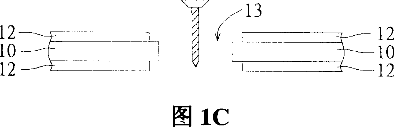
[0024] Then, an element (for example, a passive element such as a capacitor, an inductor, or a resistor) 14 is buried in the accommodating space 13, and an insulating part (ie, the first insulating layer 15 and the second insulating layer 16 mentioned later) is formed. The components 14 , the core board 10 , and the inner circuit 12 on the upper and lower sides of the core board 10 are covered. One of the possible implementation methods is as follows:

[0025] Firstly, the element 14 is arranged under the core board 10, so that the accommodating space 13 corresponds to the position of the element 14, and a first insulating layer 15 is provided under the element 14, and a second insulating layer is provided above the core board 10 16, as shown in Fig. 1D. Generally, materials that have not yet fully hardened (still have some fluidity) can be used as the first insulating layer 15 and the second insulating layer 16, so that the element 14 can be completely covered by the core bo...


PUM


Abstract

The invention discloses a method for making substrate, which includes providing a core board having inner circuits on both upper and lower sides; forming a storage space on the core board; embedding an element in the storage space and forming an insulation layer to coat the element, core board and the inner circuit of upper and lower sides; forming plural holes on the insulation layer to expose plural electrodes of the elements; forming plural through holes to drill through the insulation layer and the core board; making conductive membrane on the surface of the insulation layer and the side walls of the through holes; forming conductive layer on the conductive membrane; patterning the conductive layer to form outer layer circuit; forming anti-welding layer on the outer layer circuit.

Description

technical field [0001] The invention relates to a method for manufacturing a substrate, in particular to a method for manufacturing a substrate embedded with passive components. Background technique [0002] With the advancement of communication and electronic products, thin, light, small and high-functional products have become the mainstream trend in the market. Reducing the size and number of components used has gradually become the focus of product design and application. System in Package (SIP) has the advantages of reduced packaging area, high speed, short development time and low production cost, and has become the mainstream technology to replace traditional individual packaging systems. The whole system packaging is divided into two main axes of integrated substrate and high-density interconnection, among which the integrated substrate emphasizes the substrate [0003] With high functionality and integration features, passive components are embedded in the substrat...

Claims


Application Information

Patent Timeline
IPC IPC(8): H01L21/48H01L21/60H05K3/00
Inventor 王永辉洪清富
Owner ADVANCED SEMICON ENG INC
Why Eureka
Try Eureka