Switch controller with validation circuit for improved noise immunity

a validation circuit and controller technology, applied in the field of control circuits for semiconductor switches, can solve the problems of less effective, change in current of semiconductor switches, and interference signals, and achieve the effects of improving the shielding effect of primary windings, reducing the main inductance of transformers, and increasing capacitance coupling

Active Publication Date: 2016-01-07
POWER INTEGRATIONS INC
View PDF6 Cites 16 Cited by
  • Summary
  • Abstract
  • Description
  • Claims
  • Application Information

AI Technical Summary

Benefits of technology

[0007]The disturbances, described in detail above, as a result of increased capacitive coupling and disturbances as a result of the changes in the current through the semiconductor switch to the control circuit can occur in the second control circuit as well. Shortening the pulsed control signals can have the effect that a switching activity (switching between an ON state from an OFF state, or vice versa) of the semiconductor switch (and an associated change in the current through the semiconductor switch and the voltage across the semiconductor switch) substantially commences only after the end of the control pulse. As already described, a shielding or compensation effect of the primary winding can be more effective in this region than during a time period of an edge of the control pulses (a transition from a logic high to logic low value or vice versa). An improved shielding effect of the primary winding can thus be utilized in this time range. In addition, with the use of shorter pulses, a main inductance of the transformer can be reduced, which in turn can reduce the parasitic coupling capacitances and can thus reduce the influence of the voltage changes across the semiconductor switch. In a first embodiment, a switch controller includes a primary side comprising signal transmission circuitry to transmit signals representative of a desired transition of a switch between an on state and an off state or between an off state and an on state, the signals having a signal duration and a secondary side isolated from the primary side. The secondary side further signal reception ci...

Problems solved by technology

As a result of parasitic inductive coupling, a change in a current of the semiconductor switch can reflect back to the control circuit and generate interference signals.
Moreover, in some examples, the shielding effect of the primary winding in a specific time period around an edge of a pulsed control signal (the signal is transitioning between logic high and low values) may be less effective than in time periods in which the control signal is substantially in a steady state (the signal is substantially logic high or logic low).
That can in turn ...

Method used


Image

  • Switch controller with validation circuit for improved noise immunity
  • Switch controller with validation circuit for improved noise immunity
  • Switch controller with validation circuit for improved noise immunity

Examples


Embodiment Construction

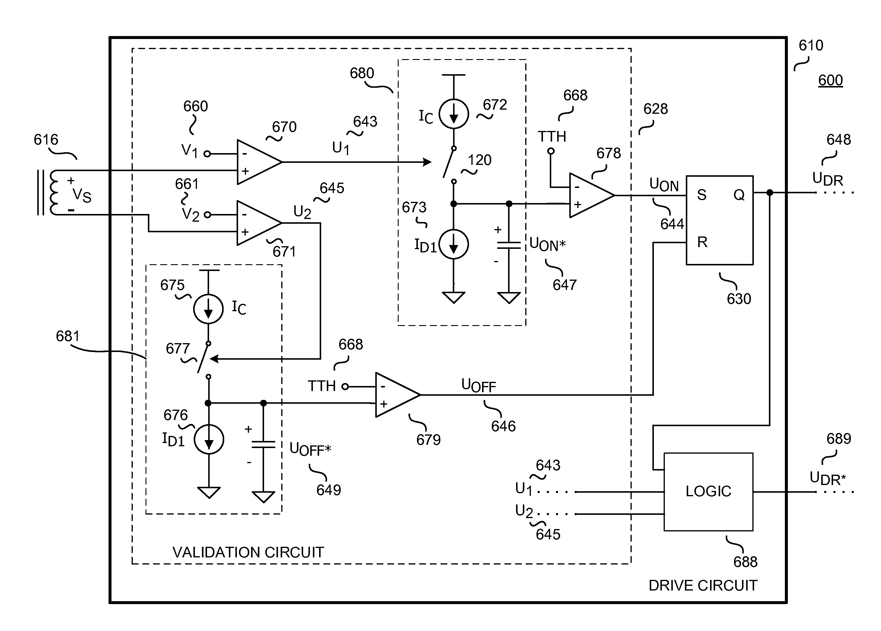
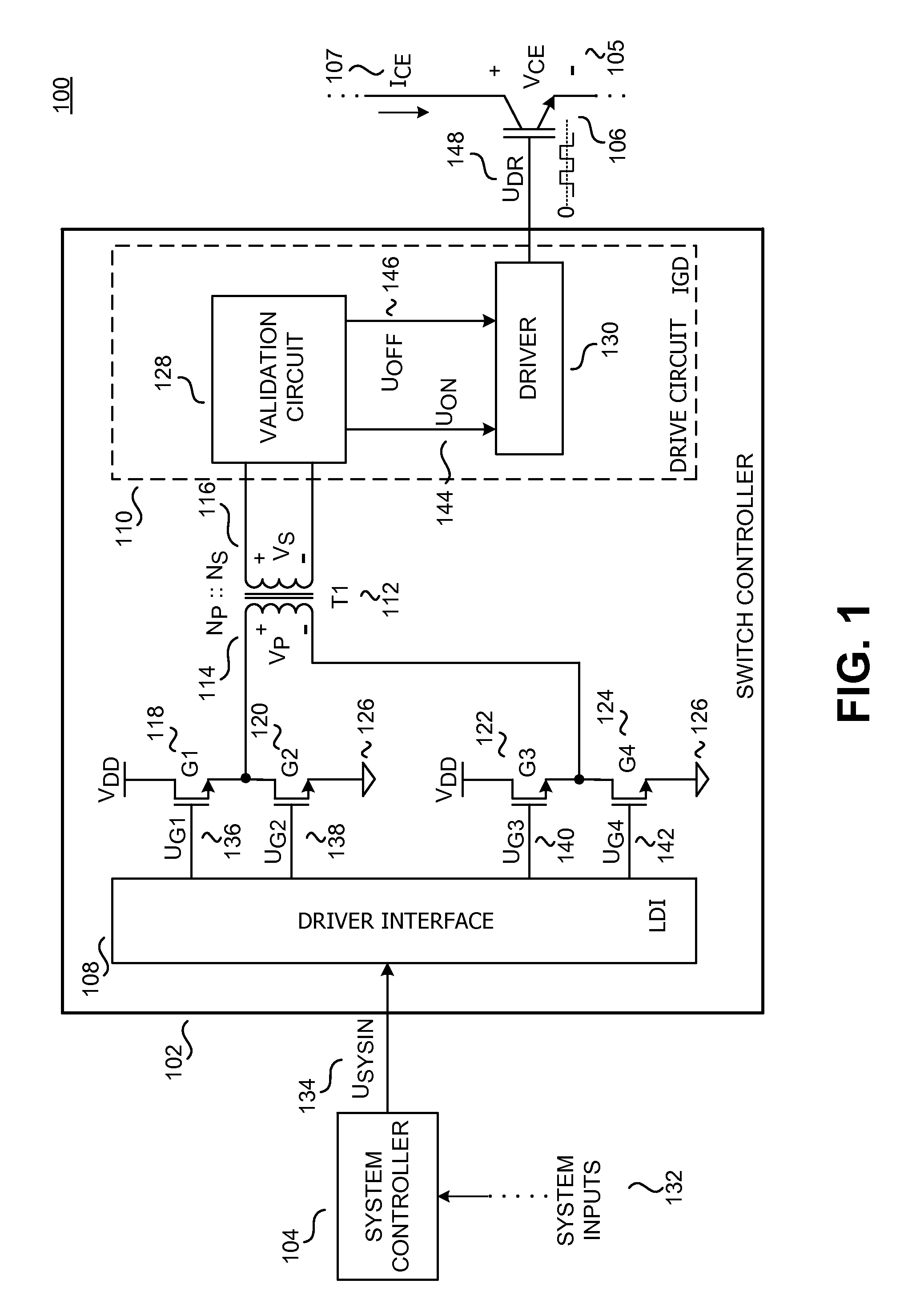
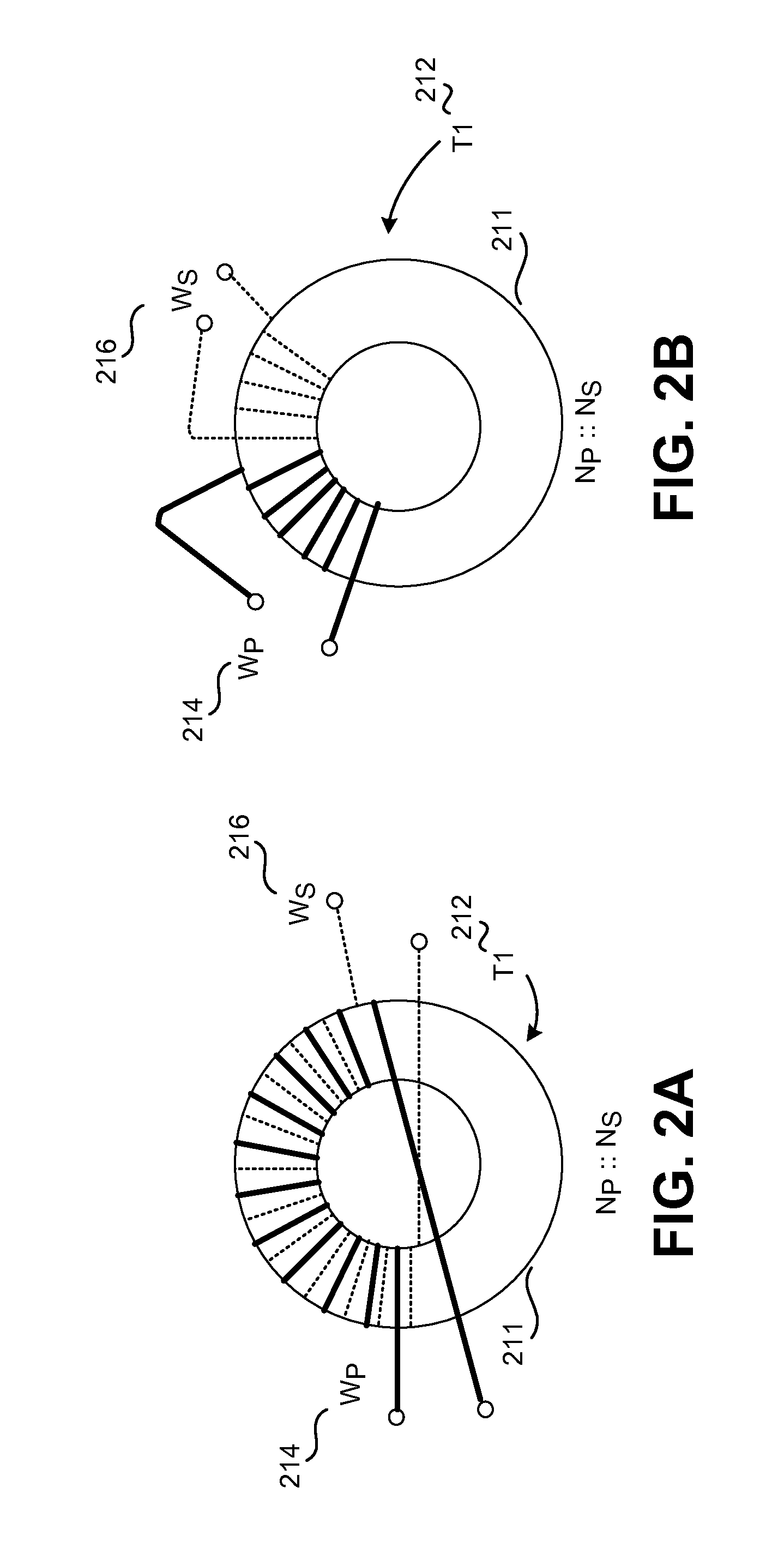
[0041]In the following description, numerous specific details are set forth in order to provide a thorough understanding of the present invention. It will be apparent, however, to one having ordinary skill in the art that the specific detail need not be employed to practice the present invention. In other instances, well-known materials or methods have not been described in detail in order to avoid obscuring the present invention. Reference throughout this specification to “one embodiment”, “an embodiment”, “one example” or “an example” means that a particular feature, structure or characteristic described in connection with the embodiment or example is included in at least one embodiment of the present invention. Thus, appearances of the phrases “in one embodiment”, “in an embodiment”, “one example” or “an example” in various places throughout this specification are not necessarily all referring to the same embodiment or example. Furthermore, the particular features, structures or ...


PUM


Abstract

A switch controller includes a primary side including signal transmission circuitry to transmit signals representative of desired transitions of a switch. A signal transformer galvanically isolates the primary side from a secondary side but inductively couples signal transmission circuitry to signal reception circuitry. A switch is coupled to switch a low impedance onto a primary side winding of the signal transformer during pauses between transmissions of the signals representative of the desired transition of the switch. The secondary side includes signal reception circuitry, a drive signal generator to generate a drive signal in response to valid signals received by the signal reception circuitry, and a validation circuit that includes a first comparator, a timer, and a second comparator to compare a timed duration with a threshold duration, and to output to the drive signal generator signals indicative of the validity of particular signals received by the signal reception circuitry.

Description

CROSS-REFERENCE TO RELATED APPLICATION[0001]This application claims the benefit of U.S. Provisional Application No. 62 / 020,864, filed Jul. 3, 2014, entitled “SWITCH CONTROLLER WITH VALIDATION CIRCUIT FOR IMPROVED NOISE IMMUNITY.”TECHNICAL FIELD[0002]The present invention relates to a control circuit for a semiconductor switch, a system having a control circuit for a semiconductor switch and at least one semiconductor switch, and a method for generating a control signal for a semiconductor switch.BACKGROUND[0003]In control circuits for semiconductor switches, in particular in control circuits for power semiconductor switches, a primary side and a secondary side can be galvanically isolated by means of an isolating transformer. That can protect the circuits at the primary side from the potentially high switched voltages on the secondary side. However, in such systems and in some situations, changes in potential at the semiconductor switch as a result of parasitic coupling capacitances...

Claims


Application Information

Patent Timeline
IPC IPC(8): H02M1/00H01F27/28H01F38/14H02M3/335
CPCH02M1/00H01F38/14H02M2001/0012H02M3/33576H01F27/2823H01F27/28H02M3/335H03K5/1252H03K17/61H03K17/691H04L25/02H04L25/0266H04L25/028H02M1/08H02M1/0012H03K17/16H03K17/56
Inventor THALHEIM, JANGARCIA, OLIVIER
Owner POWER INTEGRATIONS INC
Why Eureka
Try Eureka