Clock signal distribution with reduced parasitic loading effects

a clock signal and parasitic loading technology, applied in the direction of generating/distributing signals, pulse automatic control, electrical equipment, etc., can solve the problems of power loss and effect, load effect, jitter, etc., and achieve the effect of reducing parasitic loading

Active Publication Date: 2009-05-05
MICRON TECH INC
View PDF25 Cites 16 Cited by
  • Summary
  • Abstract
  • Description
  • Claims
  • Application Information

AI Technical Summary

Benefits of technology

[0004]It is an object of this invention to provide clock signal distribution systems with reduced parasitic loading effects.
[0005]In accordance with this invention, a clock signal distribution system is provided in which a reference clock signal is frequency-divided prior to being distributed over a long trace to one or more digital sub-systems. A frequency divider outputs a clock signal having a lower frequency than the reference clock frequency. A delay-locked loop (DLL) circuit “locks” to the lower frequency signal, and outputs a corresponding lower frequency clock signal for distribution over the trace. Power loss through the characteristic capacitive load of the trace is thereby reduced. Parasitic effects associated with clock jitter are also reduced. A frequency multiplying phase-locked loop (PLL) circuit locks to the lower frequency clock signal and outputs at least one clock signal having a higher frequency than the frequency of the lower frequency signal (e.g., outputs a signal having a frequency equal to the reference clock frequency). Multi-phase clock signals may be optionally generated by the PLL.
[0006]In some embodiments, the time required for a frequency-multiplying PLL of the invention to lock to an input signal is advantageously reduced. A frequency-multiplying PLL having voltage-controlled delay units (VCDs) is initialized with the control voltage of a DLL having substantially identical VCDs. In general, DLLs have characteristically faster lock times than do PLLs. The DLL receives the reference clock signal as input. The control voltage of the DLL is provided to the PLL, and causes the PLL to lock to a desired frequency at substantially the same time that the DLL locks. Once the PLL is locked, the control voltage that maintains the frequency lock of the PLL is locally generated by the PLL.
[0007]The invention also provides methods of distributing clock signals with reduced parasitic loading effects.

Problems solved by technology

The parasitic capacitances result in loading effects (e.g., power loss and effects associated with clock jitter) that can vary in direct proportion to both clock frequency and trace length.
Technology trends indicate that the physical separation of system clock generators and associated digital sub-systems will increase as digital circuits become progressively more complex, thereby resulting in increased parasitic load.
Moreover, the effects of parasitic loading in digital systems are further exacerbated by ever-increasing system clock frequency.

Method used


Image

  • Clock signal distribution with reduced parasitic loading effects
  • Clock signal distribution with reduced parasitic loading effects
  • Clock signal distribution with reduced parasitic loading effects

Examples


Embodiment Construction

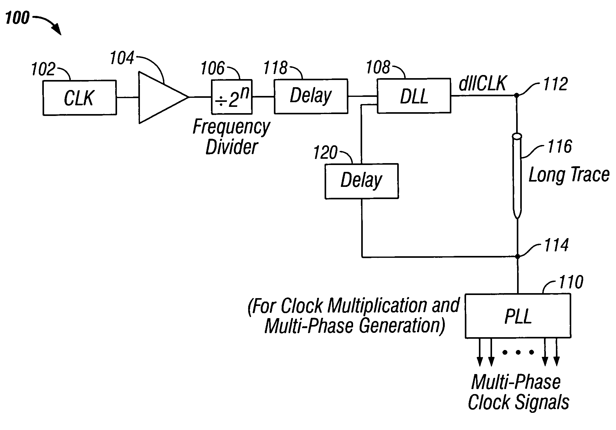
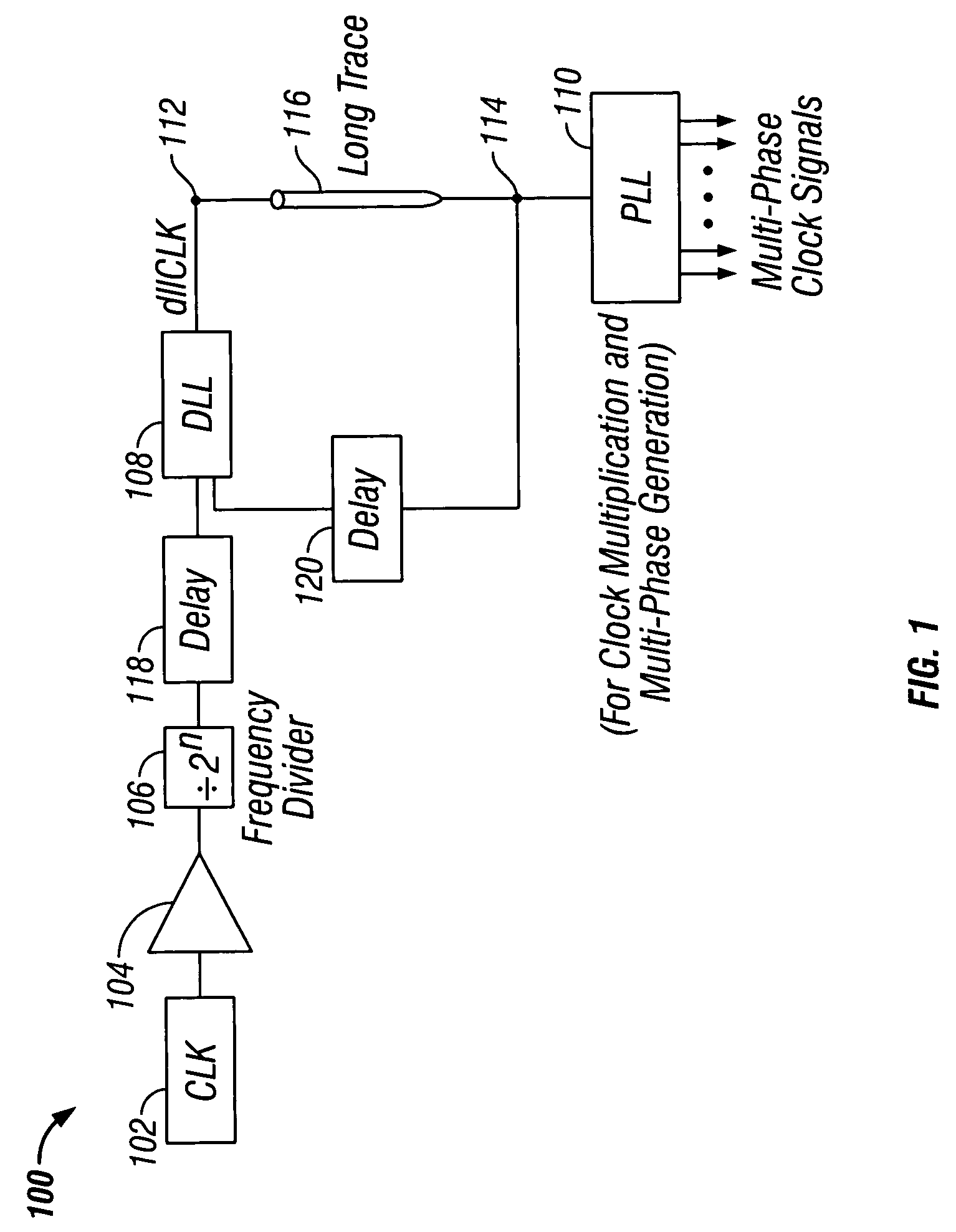
[0014]The invention is directed to reducing parasitic loading effects in clock signal distribution systems.

[0015]FIG. 1 shows a clock signal distribution system 100 in accordance with the invention. System 100 includes clock generator 102, buffer 104, frequency divider 106, delay-locked loop (DLL) 108 and phase-locked loop (PLL) 110. Clock generator 102 outputs a reference clock signal having a first frequency (fref) to buffer 104. Frequency divider 106 receives the reference clock signal from buffer104, and outputs to DLL 108 a second clock signal having a frequency (f2) that is equal to the reference clock frequency divided by 2n (i.e., f2=fref / 2n) for all positive integers n. DLL 108“locks” to the second clock signal and outputs at output 112 a third clock signal preferably having the same frequency (f2) as the second clock signal. Other frequencies may of course be provided by DLL 108. “Locking” by DLL and PLL circuits is described in greater detail below in connection with FIGS...


PUM


Abstract

Clock signal distribution systems with reduced parasitic loading effects are provided. A reference clock is frequency-divided to produce a lower frequency clock signal. A delay-locked loop (DLL) circuit locks to the lower frequency clock signal, and outputs a corresponding lower frequency clock signal for distribution over a long trace. Power consumption caused by parasitic capacitance of the trace is thereby reduced. Parasitic effects associated with clock jitter are also reduced. A frequency multiplying phase-locked loop (PLL) circuit locks to the lower frequency clock signal, and outputs at least one clock signal having a higher frequency than the lower frequency signal.

Description

BACKGROUND OF THE INVENTION[0001]This invention relates to clock signal distribution systems. More particularly, this invention relates to clock signal distribution systems with reduced parasitic loading effects.[0002]System clock signals are typically remotely generated for distribution to various digital circuit subsystems. The system clock generator and the digital subsystems may be located in geographically disparate regions of the digital circuit. Clock signals are distributed throughout the digital circuit over traces (i.e., device interconnects; e.g., a signal wire) having characteristic parasitic capacitances. The parasitic capacitances result in loading effects (e.g., power loss and effects associated with clock jitter) that can vary in direct proportion to both clock frequency and trace length. Technology trends indicate that the physical separation of system clock generators and associated digital sub-systems will increase as digital circuits become progressively more com...

Claims


Application Information

Patent Timeline
Patent Type & Authority Patents(United States)
IPC IPC(8): H03L7/06G06F1/10H03L7/07H03L7/081H03L7/099
CPCG06F1/10H03L7/07H03L7/0812H03L7/0995H03L7/0816
Inventor LEE, SEONG-HOONLIN, FENG
Owner MICRON TECH INC
Why Eureka
Try Eureka