Active array substrate, liquid crystal display panel and method for manufacturing active array substrate

An active array and substrate technology, applied in semiconductor/solid-state device manufacturing, optics, instruments, etc., can solve problems affecting display quality and inconsistency, achieve the effect of improving display quality and avoiding uneven load effect

Active Publication Date: 2009-10-21
AU OPTRONICS CORP
View PDF1 Cites 12 Cited by
  • Summary
  • Abstract
  • Description
  • Claims
  • Application Information

AI Technical Summary

Problems solved by technology

When the loading effect is not uniformly generated on each pixel, the effect on each pixel...

Method used


Image

  • Active array substrate, liquid crystal display panel and method for manufacturing active array substrate
  • Active array substrate, liquid crystal display panel and method for manufacturing active array substrate
  • Active array substrate, liquid crystal display panel and method for manufacturing active array substrate

Examples


no. 1 example

[0060] Figure 2A to Figure 2G It is a flow chart of the manufacturing method of the active array substrate according to the first embodiment of the present invention.

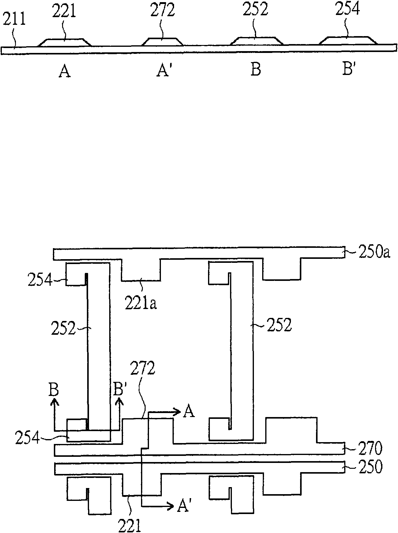
[0061] Please refer to Figure 2AFirstly, a substrate 211 is provided, a first conductive layer (not shown) is formed on the substrate 211, and then the first conductive layer is patterned to form scanning lines 250, 250a, gates 221, 221a, common lines 270, and capacitor lower electrodes 272 , the first part 252 and the transfer part 254 . The way of patterning the first conductive layer can be known methods such as exposure, development and etching, for example. The wire transfer part 254 is connected to the first part 252. For a pixel unit, both ends of the first part 252 can be respectively connected to a wire transfer part 254, that is, the first part 252 and the two wire transfer parts 254 can be roughly Constitute a reverse C-shaped or I-shaped, but not limited to this. The capacitor bottom electrode...

no. 2 example

[0071] image 3 It is the active array substrate of the second embodiment of the present invention.

[0072] Please refer to image 3 , the only difference from the first embodiment is that only a part of the auxiliary semiconductor layer 282 and the data line 290 overlaps with the first portion 252 , so as to reduce the load effect slightly. The remaining components and manufacturing methods are the same or similar to those of the first embodiment, and will not be repeated here.

no. 3 example

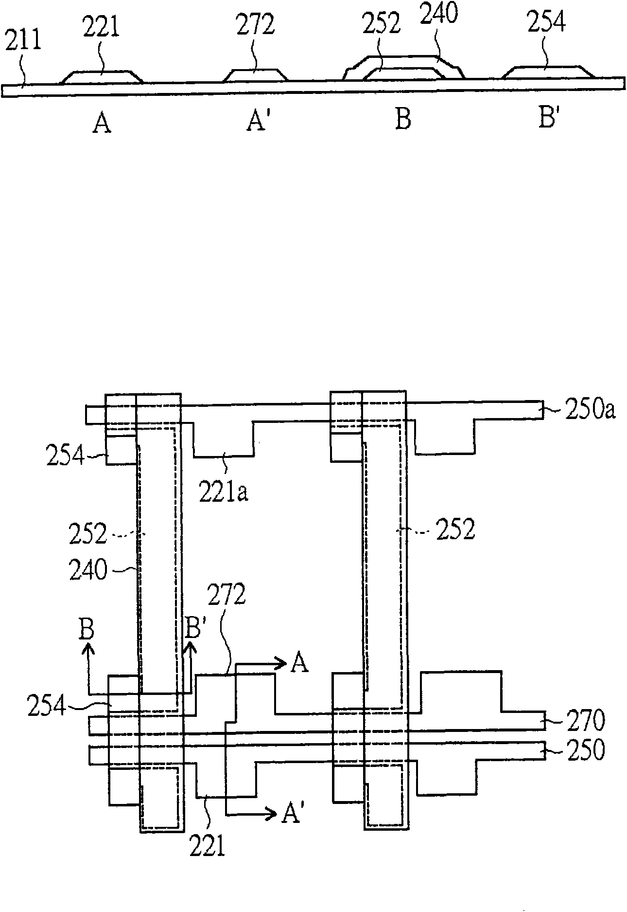
[0074] Figure 4 It is the active array substrate of the third embodiment of the present invention.

[0075] Please refer to Figure 4 , the only difference from the first embodiment is that the auxiliary semiconductor layer 282 and the data line 290 are completely offset from the first portion 252 and do not overlap, so as to reduce the load effect. The remaining components and manufacturing methods are the same or similar to those of the first embodiment, and will not be repeated here.


PUM


Abstract

The invention provides an active array substrate, a liquid crystal display panel and a method for manufacturing the active array substrate. The active array substrate comprises a substrate, a plurality of scanning lines, a plurality of data wires and a plurality of grid electrode patch cords arranged on the substrate, wherein the grid electrode patch cords have a plurality of first parts, a plurality of patch cord parts connected with the corresponding first parts, a plurality of connection holes and a plurality of second parts. The second parts and the first parts are not arranged at the same layer and one of the second parts is electrically connected with the corresponding first part by one of the connection holes.

Description

technical field [0001] The present invention relates to an active array substrate, a liquid crystal display panel and a method for manufacturing the active array substrate, in particular to a narrow-frame active array substrate with uniform imaging, a liquid crystal display panel, and a narrow-frame active array substrate with uniform imaging Manufacturing method. Background technique [0002] Flat Panel Display (FPD) is currently the main popular display, among which liquid crystal display panels are widely used in computer screens, mobile phones, personal digital assistants (PDAs) because of their thin and light appearance, power saving and no radiation. ), flat-screen TVs and other electronic products. The working principle of the liquid crystal display panel is to change the alignment state of the liquid crystal molecules in the liquid crystal layer by changing the voltage difference between the two ends of the liquid crystal layer to change the light transmittance of t...

Claims


Application Information

Patent Timeline
IPC IPC(8): G02F1/1362H01L23/528H01L21/82H01L21/768
Inventor 陈昱丞王参群陈茂松
Owner AU OPTRONICS CORP
Why Eureka
Try Eureka