Chip resistor

a chip resistor and resistance value technology, applied in resistors, resistor details, electrical equipment, etc., can solve the problems that the resistance value that would inhibit the chip resistor from lowering its resistance is unavoidably generated by the end-face electrode, and the inductance of the end-face electrode cannot be ignored, so as to improve the tcr characteristics, and reduce the probability of mounting failure

Inactive Publication Date: 2010-08-24
KOA CORP
View PDF11 Cites 33 Cited by
  • Summary
  • Abstract
  • Description
  • Claims
  • Application Information

AI Technical Summary

Benefits of technology

[0011]The chip resistor according to the present invention has the first and second electrode layers, which are formed over the bank-raising foundation sections on the lower surface of the ceramic substrate. Therefore, the outermost layer of the plating layer covering the second electrode layers can easily protrude downward from the protective layer covering the resistive element. As a result, it is unlikely that the chip resistor will be inclined when mounted on the circuit board. This decreases the probability of mounting failure. Further, the chip resistor has a resistive element made of a low-resistance, low-TCR material. Further, when it is face-down mounted, it can distribute power to the resistive element while bypassing the end-face electrodes. Furthermore, the electrode section (which includes the first and second electrode layers) for the resistive element has a two-layer structure and accepts an extremely small inductance setting. Therefore, the chip resistor can readily lower its resistance and improve TCR characteristics. In addition, when the chip resistor is mounted on a circuit board, the end-face electrodes create a solder fillet. This makes it easy to obtain required mounting strength.

Problems solved by technology

Therefore, when an attempt is made to lower the resistance of the chip resistor, the inductance of the end-face electrode cannot be ignored.
Therefore, a resistance value that would inhibit the chip resistor from lowering its resistance is unavoidably generated by the end-face electrode.

Method used


Image

  • Chip resistor
  • Chip resistor
  • Chip resistor

Examples


Embodiment Construction

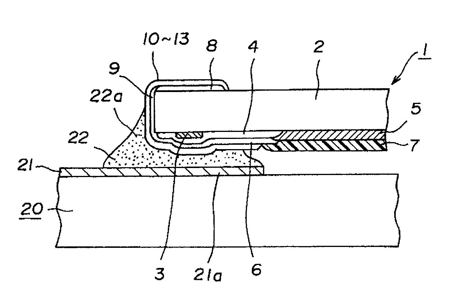
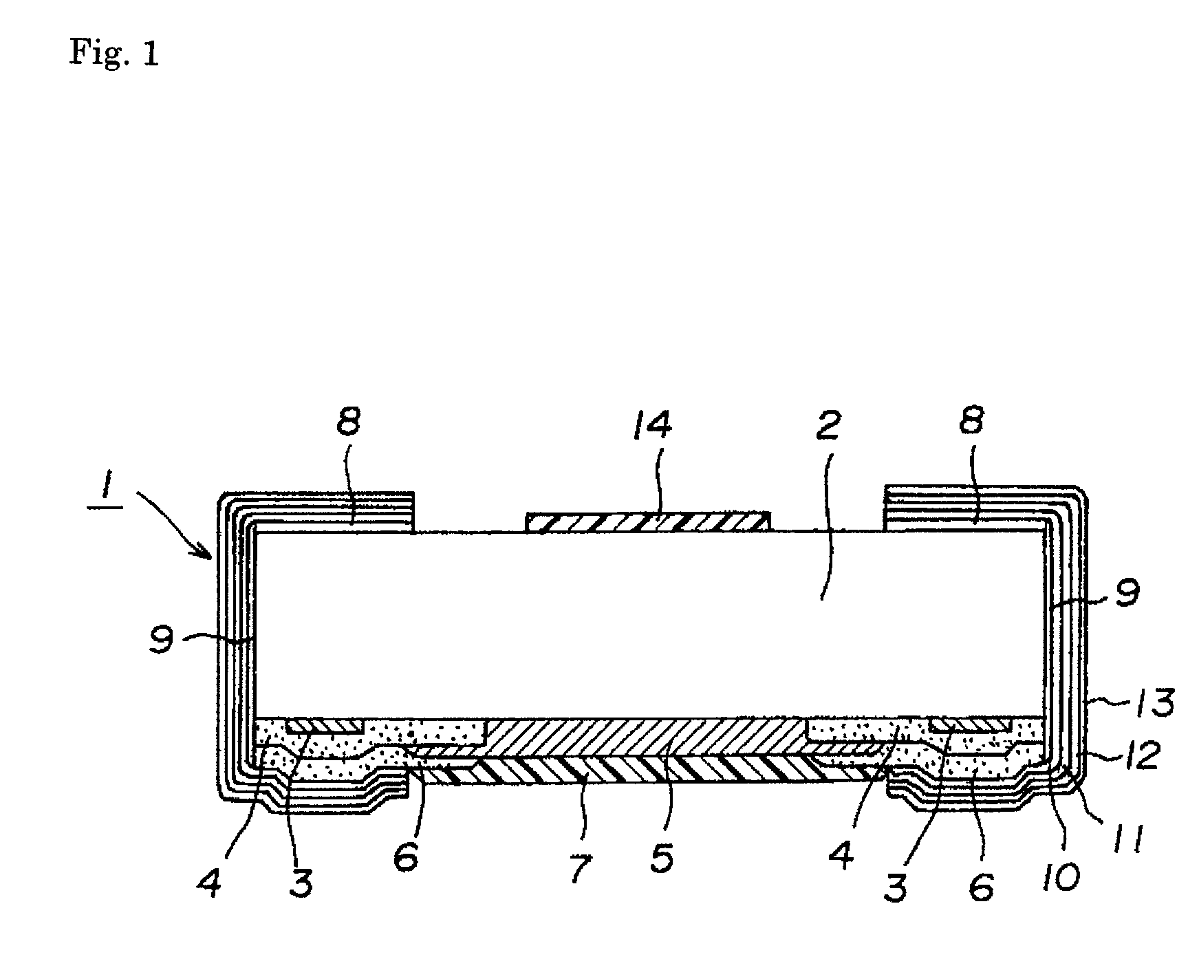
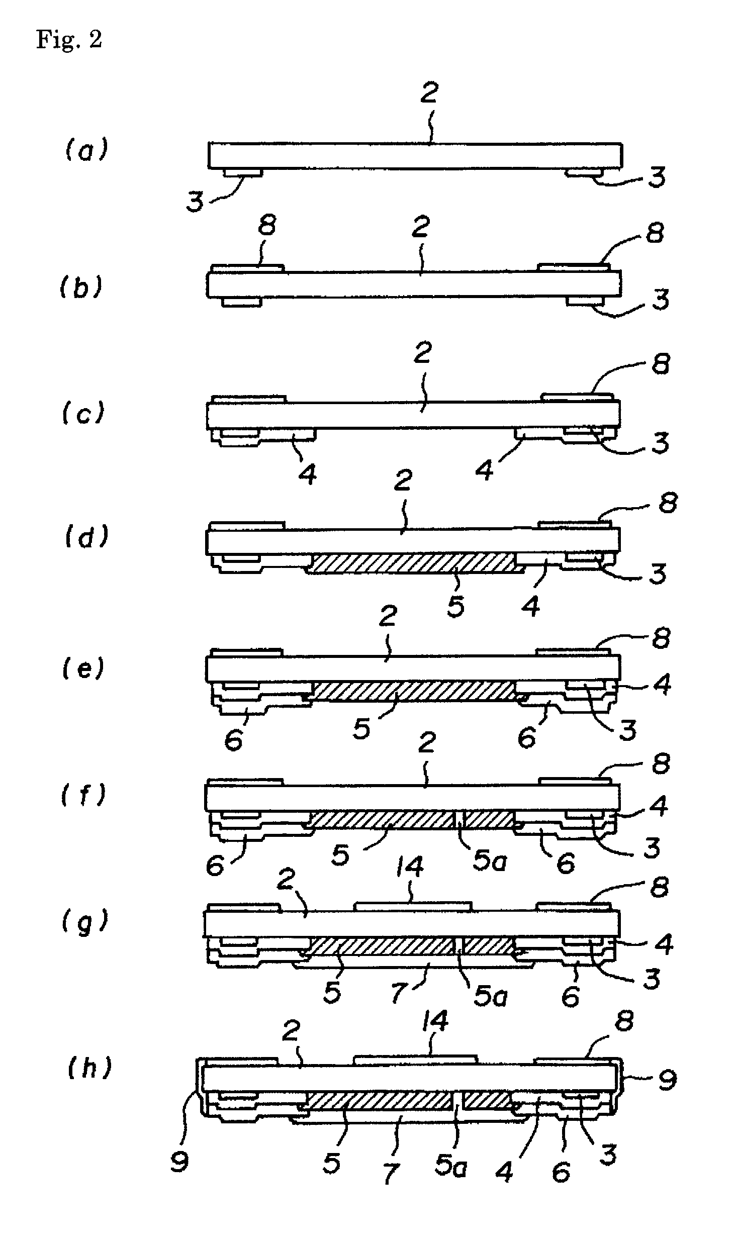
[0012]Embodiments of the present invention will now be described with reference to the accompanying drawings. FIG. 1 is a cross-sectional schematic view illustrating a chip resistor according to an embodiment of the present invention. FIG. 2 is a cross-sectional view illustrating a manufacturing process for the chip resistor. FIG. 3 is a plan view illustrating a manufacturing process for the chip resistor. FIG. 4 is a cross-sectional view illustrating an essential part of the chip resistor mounted on a circuit board.

[0013]The chip resistor 1 shown in the above figures is of a low-resistance, low-TCR type and is to be face-down mounted on a circuit board 20. This chip resistor 1 includes a ceramic substrate 2 that is shaped like a rectangular parallelepiped. Mounted on the lower surface of the ceramic substrate 2 are a pair of bank-raising foundation sections 3 that are made mainly of glass, a pair of trapezoidal first electrode layers 4 that cover parts of the bank-raising foundatio...


PUM


Abstract

Disclosed is a chip resistor 1 that includes a ceramic substrate 2, a pair of bank-raising foundation sections 3 positioned on both longitudinal ends of the lower surface of the ceramic substrate 2, a pair of first electrode layers 4 that cover at least parts of the bank-raising foundation sections 3 and are positioned at a predetermined distance from each other, a resistive element 5 that is made mainly of a copper-nickel alloy to bridge the first electrode layers 4, a pair of second electrode layers 6 that cover the pair of first electrode layers 4, and an insulating protective layer 7 that covers the resistive element 5. Further, end-face electrodes 9 are positioned on both longitudinal end faces of the ceramic substrate 2. The second electrode layers 6 and end-face electrodes 9 are covered with plating layers 10-13. This chip resistor 1 is to be face-down mounted with the first and second electrodes 4, 6 positioned on a wiring pattern 21 of a circuit board 20.

Description

TECHNICAL FIELD[0001]The present invention relates to a low-resistance chip resistor that is used, for instance, for current detection in an electronic circuit, and more particularly to a low-resistance chip resistor that is to be face-down mounted.BACKGROUND ART[0002]A common chip resistor is made by providing the upper surface of a ceramic substrate with a pair of upper electrodes, a resistive element for bridging the upper electrodes, and a protective layer for covering the resistive element, providing the lower surface of the ceramic substrate with a pair of lower electrodes, and providing both longitudinal end faces of the ceramic substrate with an end-face electrode. The end-face electrode is closely attached to the upper and lower electrodes. Each of these electrodes is covered with a plating layer. When the chip resistor is to be mounted, the lower electrodes are positioned on a wiring pattern of a circuit board, and then the wiring pattern is soldered to the plating layer s...

Claims


Application Information

Patent Timeline
Patent Type & Authority Patents(United States)
IPC IPC(8): H01C1/012
CPCH01C1/012H01C1/142H01C7/003
Inventor URANO, KOICHI
Owner KOA CORP
Why Eureka
Try Eureka