Liquid crystal display device and method for manufacturing the same

a technology of liquid crystal display and liquid crystal, which is applied in the direction of semiconductor devices, instruments, electrical devices, etc., can solve the problems that the manufacturing process cannot be prevented from being complicated, and achieve the effect of simplifying the manufacturing process and improving the efficiency of materials

Inactive Publication Date: 2010-09-14
SEMICON ENERGY LAB CO LTD
View PDF32 Cites 35 Cited by
  • Summary
  • Abstract
  • Description
  • Claims
  • Application Information

AI Technical Summary

Benefits of technology

[0008]In particular, as a substrate that is to be a base material gets larger, time of manufacture is increased due to the repetition of film formation and etching; waste disposal costs of etchant and the like are increased; and material efficiency is significantly reduced.
[0009]In view of the above problems, it is an object of the present invention to provide a manufacturing method of an electro-optical device by which the manufacturing cost can be reduced.
[0012]In addition, the invention provides a technology for easily obtaining an electrical connection between multi-layer wirings.
[0025]According to the invention, a material layer can be patterned without using a photo mask; thus, the material efficiency can be improved. Further, the manufacturing process can be simplified by skipping the steps of exposure and development in manufacturing a liquid crystal display device.

Problems solved by technology

Therefore, the manufacturing process can not be prevented from being complicated.

Method used


Image

  • Liquid crystal display device and method for manufacturing the same
  • Liquid crystal display device and method for manufacturing the same
  • Liquid crystal display device and method for manufacturing the same

Examples


embodiment mode 1

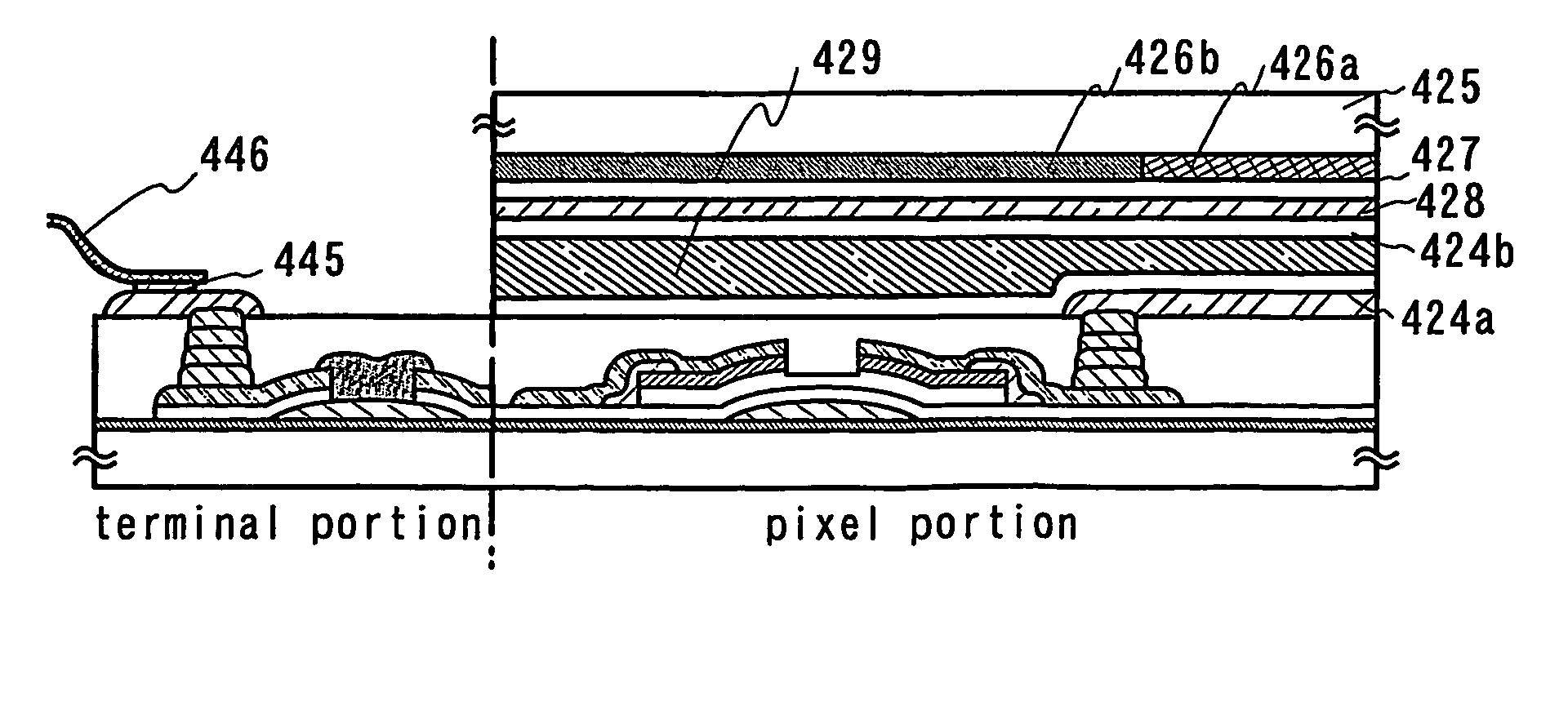
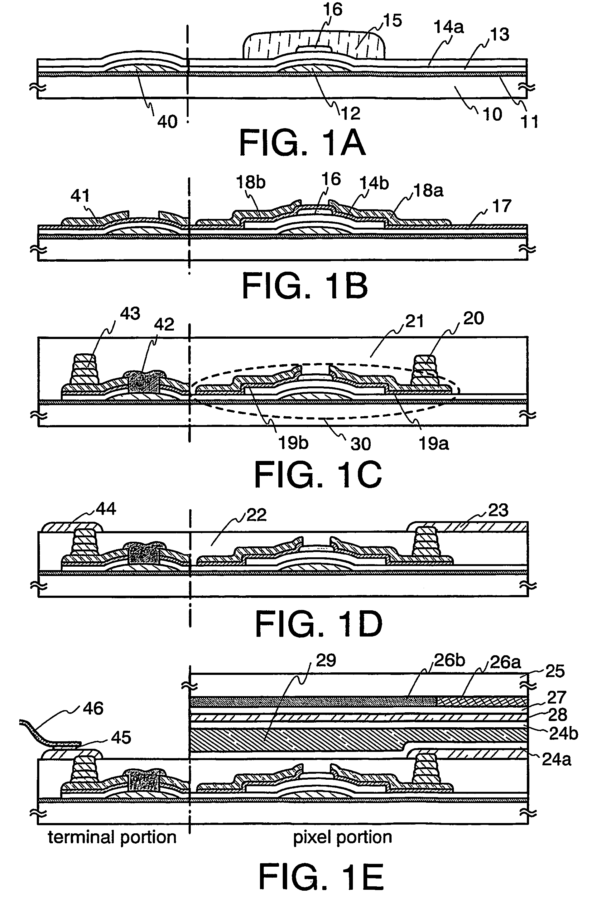
[0048]Here, a method for manufacturing an active matrix liquid crystal display device using an inverted staggered TFT as a switching element will be described. FIG. 1 shows a cross section of the manufacturing process.

[0049]First, a base film 11 for improving adhesion with a material layer to be later formed by a droplet discharge method is formed over a substrate 10. The base film 11 may be formed thin; accordingly, it can be regarded as base pretreatment. A photocatalyst (titanium oxide (TiO2), strontium titanate (SrTiO3), cadmium selenide (CdSe), potassium tantalate (KTaO3), cadmium sulfide (CdS), zirconium oxide (ZrO2), niobium oxide (Nb2O5), zinc oxide (ZnO), iron oxide (Fe2O3), tungsten oxide (WO3)) may be applied with a spray; alternatively, an organic material (polyimide, acryl, or a material having a skeletal structure including a bond of silicon (Si) and oxygen (O) which contains at least one of the group consisting of hydrogen, fluorine, alkyl group and aromatic hydrocarb...

embodiment mode 2

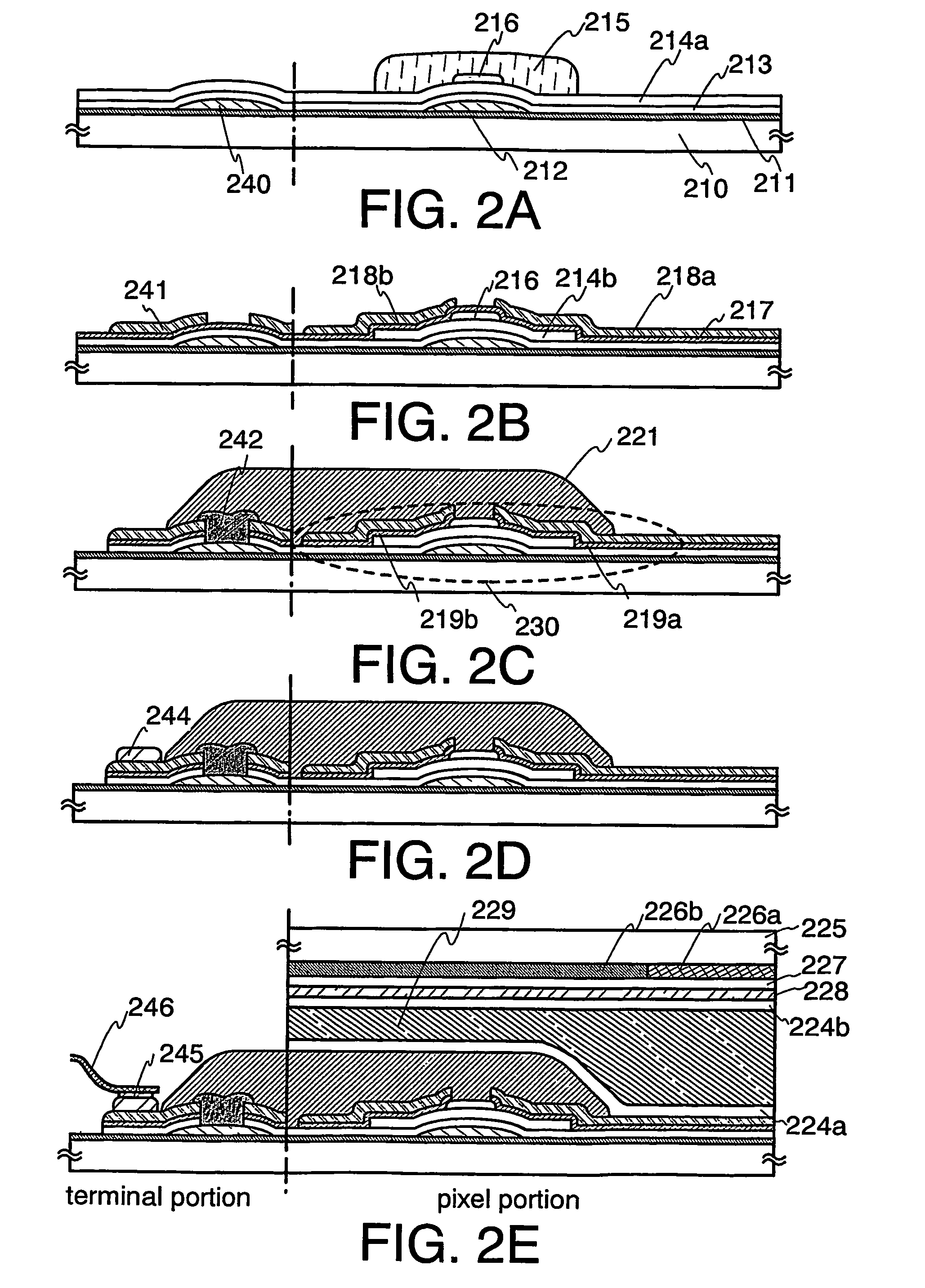
[0093]Here, an example in which the connection method is different from Embodiment Mode 1 will be shown. FIG. 2A to 2E show a cross section of manufacturing steps of an active matrix liquid crystal display device using an inverted staggered TFT as a switching element.

[0094]First, a state equivalent to FIG. 1A is made according to the steps shown in Embodiment Mode 1. A base film 211, a metal wiring 212, a wiring 240 extending to a terminal area are formed over a substrate 210. Further, a gate insulating film 213, a semiconductor film 214a, and an insulating layer 216 are sequentially formed thereover. A mask 215 covering the insulating layer 216 is formed by a droplet discharge method (FIG. 2A).

[0095]Next, a semiconductor film 214a except the area covered with the mask 215 is removed by dry etching or wet etching, so that a semiconductor layer 214b to be an active layer is formed.

[0096]After the mask 215 is removed, an n-type semiconductor film 217 is formed over the entire surface....

embodiment mode 3

[0114]Here, an example in which the connection method is different from Embodiment Mode 1 will be shown. FIGS. 3A to 3D show a cross section of manufacturing steps of an active matrix liquid crystal display device using an inverted staggered TFT as a switching element.

[0115]First, a state equivalent to FIG. 1C is made according to the steps shown in Embodiment Mode 1. A base film 311, a metal wiring 312, a wiring 340 extending to a terminal area are formed over a substrate 310. Further, a gate insulating film 313, a semiconductor film, and an insulating layer 316 are sequentially formed thereover. A mask covering the insulating layer 316 is formed by a droplet discharge method. Next, a semiconductor film except the area covered with the mask is removed by dry etching or wet etching, so that a semiconductor layer 314 to be an active layer is formed. After the mask is removed, an n-type semiconductor film is formed over the entire surface. Next, a composition-containing a conductive m...


PUM

PropertyMeasurementUnit
thicknessaaaaaaaaaa
grain diameteraaaaaaaaaa
wavelengthaaaaaaaaaa

Abstract

As a substrate gets larger, time of manufacture is increased due to the repetition of film formations and etchings; waste disposal costs of etchant and the like are increased; and material efficiency is significantly reduced. A base film for improving adhesion between a substrate and a material layer formed by a droplet discharge method is formed in the invention. Further, a manufacturing method of a liquid crystal display device according to the invention includes at least one step for forming the following patterns required for manufacturing a liquid crystal display device without using a photomask: a pattern of a material layer typified by a wiring (or an electrode) pattern, an insulating layer pattern; or a mask pattern for forming another pattern.

Description

TECHNICAL FIELD[0001]The present invention relates to a semiconductor device having a circuit that is composed of a thin film transistor (hereinafter referred to as TFT) and a method for manufacturing the semiconductor device. An example of the semiconductor device is electronic device having an electro-optical device typified by a liquid crystal display device as one of its parts.[0002]In this specification, the term semiconductor device refers to devices that function by utilizing semiconductor characteristics. Further, electro-optical devices, semiconductor circuits, and electronic devices are all regarded as semiconductor devices.BACKGROUND ART[0003]In late years, a technology for forming a thin film transistor (TFT) using a semiconductor thin film (a thickness of around several nanometers to several hundred nanometers) formed over a substrate having an insulating surface has been attracting attention. Thin film transistors are broadly applied to electronic devices such as an IC...

Claims


Application Information

Patent Timeline
Patent Type & Authority Patents(United States)
IPC IPC(8): H01L31/00G02F1/1339G02F1/1362G02F1/1368H01L21/288
CPCG02F1/13458G02F1/136227H01L27/1292G02F1/136286G02F2001/13415G02F2001/136295G02F1/13415G02F1/136295G02F1/136
Inventor YAMAZAKI, SHUNPEIMAEKAWA, SHINJIFUJII, GENKUWABARA, HIDEAKI
Owner SEMICON ENERGY LAB CO LTD
Why Eureka
Try Eureka